

20206-08-28 慶應義塾大学,理化学研究所
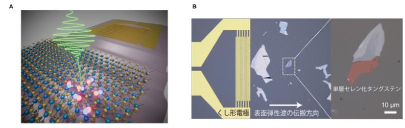
(A) 表面弾性波による原子層二次元半導体の励起子発光変調の模式図. (B) 作製した表面弾性波デバイスと単層セレン化タングステンの顕微鏡写真.
<関連情報>
- https://www.keio.ac.jp/fixed-files/20260828-press-01-k9wn3hvx.pdf
- https://www.science.org/doi/10.1126/sciadv.aef5458
二次元半導体における伝搬音響歪み下での励起子ダイナミクスの多次元スペクトル時間イメージング Multidimensional spectro-temporal imaging of exciton dynamics under propagating acoustic strain in two-dimensional semiconductors
Yuta Takahashi, Takumi Yamamoto Hidetoshi Kanzawa, Kazuki Maezawa, […] , and Shun Fujii
Science Advances Published:21 Aug 2026
DOI:https://doi.org/10.1126/sciadv.aef5458
Abstract
Dynamic strain offers a promising route to manipulate tightly bound excitons in two-dimensional semiconductors. Its impact, however, has so far been inferred primarily from time-averaged or spatially integrated measurements. In particular, for dynamic strain driven by surface acoustic waves (SAWs), the relatively small strain amplitude and competing piezoelectric effects have hindered direct access to the real-time evolution of exciton emission energy and recombination dynamics within a single acoustic cycle. Here we report a fully phase-synchronized, multidimensional spectro-temporal-spatial visualization of exciton emission in monolayer tungsten diselenide driven by propagating SAWs. By integrating phase-resolved microscopy and interferometric surface displacement measurements, we achieve simultaneous mapping of exciton emission energy, photoluminescence intensity, linewidth, and decay dynamics and directly correlate them with the dynamic strain field. Our work establishes propagating acoustic strain as a powerful platform for deterministic exciton control and provides a comprehensive framework for exploring nonequilibrium exciton dynamics in low-dimensional materials.

