")
2022-02-03 米国国立標準技術研究所(NIST)
米国国立標準技術研究所(NIST)の研究者たちは、スマートフォンやコンピュータなど現代の電子機器の構成要素であるトランジスタの欠陥を特定し、カウントするための、かつて信頼されていた技術を復活させ、改良しました。過去10年間で、高性能コンピュータチップのトランジスタ部品は非常に小さくなり、チャージポンプとして知られる一般的な方法では、欠陥を正確に数えることができなくなった。NISTの新しく改良された方法は、最新の極小技術に十分な感度を持ち、そうでなければトランジスタの性能を損ない、トランジスタが搭載されたチップの信頼性を制限する可能性がある欠陥を正確に評価することができる。
A traditional method gets a new lease on life and may provide a new standard for measuring electric current.
Researchers at the National Institute of Standards and Technology (NIST) have revived and improved a once-reliable technique to identify and count defects in transistors, the building blocks of modern electronic devices such as smartphones and computers. Over the past decade, transistor components have become so small in high-performance computer chips that the popular method, known as charge pumping, could no longer count defects accurately. NIST’s new and improved method is sensitive enough for the most modern, minuscule technology, and can provide an accurate assessment of defects that could otherwise impair the performance of transistors and limit the reliability of the chips in which they reside.
The new, modified charge pumping technique can detect single defects as small as the diameter of a hydrogen atom (one-tenth of a billionth of a meter) and can indicate where they’re located in the transistor. Researchers could also use the new capability to detect and manipulate a property in each electron known as quantum spin. The ability to manipulate individual spins has applications in both basic research and quantum engineering and computing.
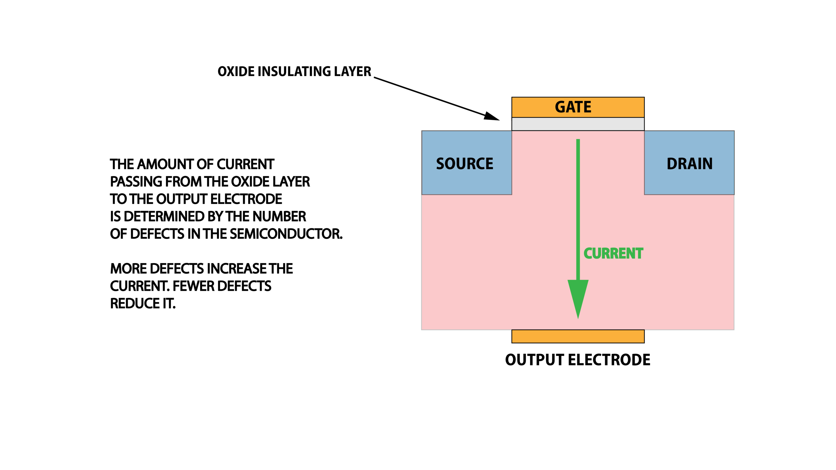
Transistors act as electrical switches. In the on position, which represents the “1” of binary digital information, a designated amount of current flows from one side of a semiconductor to the other. In the off position, representing the “0” of binary logic, current ceases to flow.
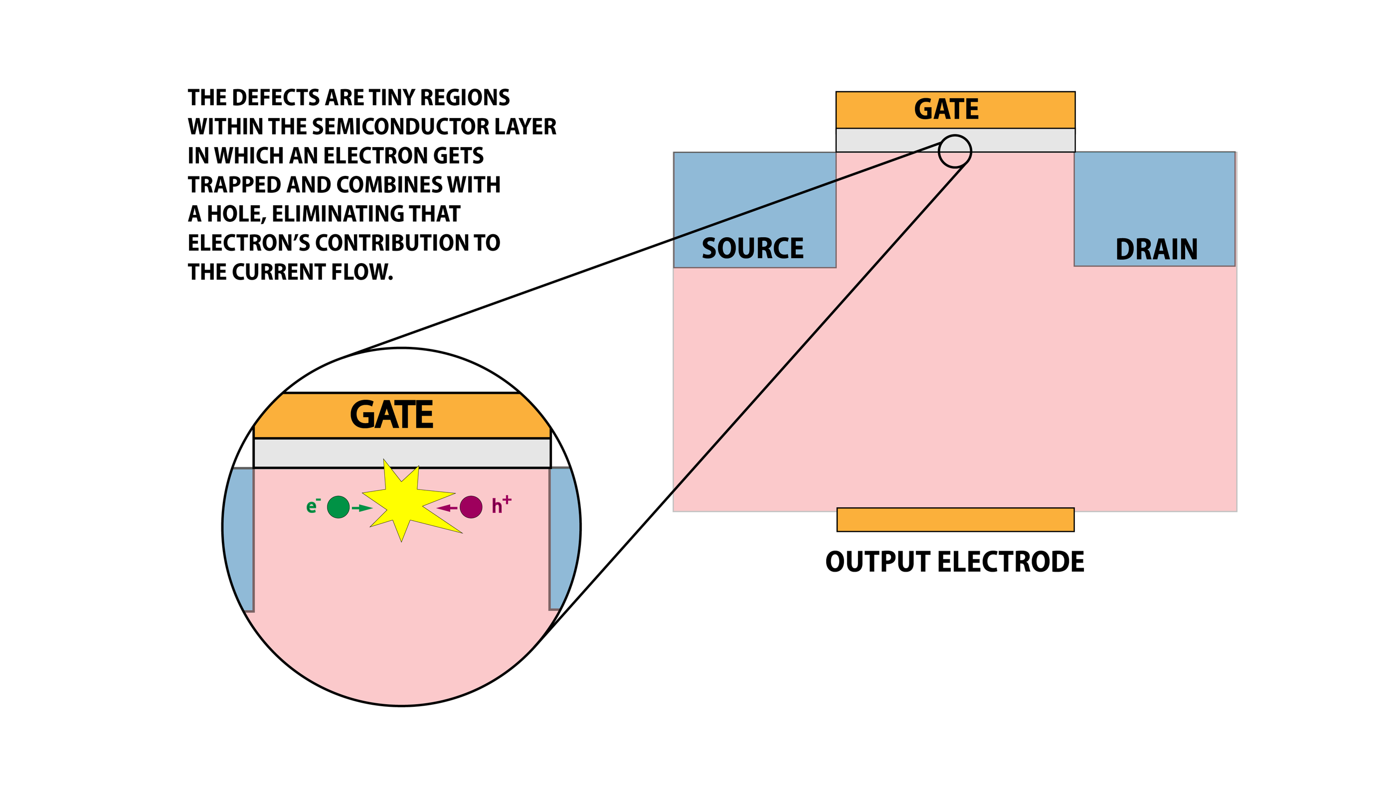
Defects in a transistor can interfere with the reliable flow of current and significantly degrade the performance of transistors. These defects could be broken chemical bonds in the transistor material. Or they could be atomic impurities that trap electrons in the material. Scientists have devised several ways to categorize defects and minimize their impact, tailored to the structure of the transistor under study.
In the traditional design known as the metal oxide semiconductor field effect transistor (MOSFET), a metal electrode called the gate sits atop a thin insulating layer of silicon dioxide. Below the insulating layer lies the interface region that separates the insulating layer and the main body of the semiconductor. In a typical transistor, current travels through a narrow channel, only one billionth of a meter thick, that extends from the source, which lies on one side of the gate, to a “drain” on the other side. The gate controls the amount of current in the channel.
")
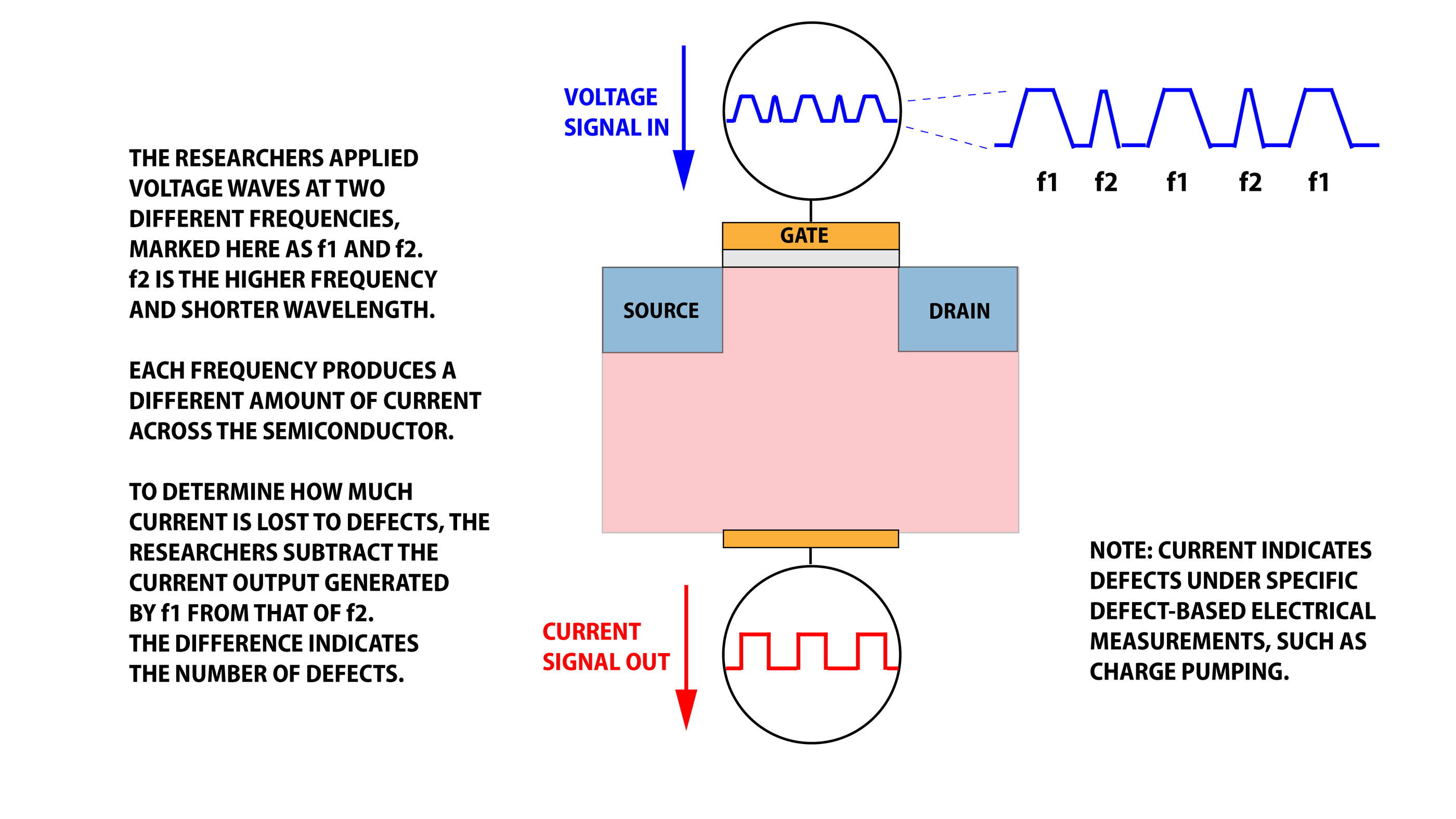
Charge pumping is a two-step process in which the examiner alternately pulses the gate with a positive test voltage, then a negative one. (The transistor does not act as an on/off switch during this testing mode.) In traditional charge pumping, the alternating voltage pulses are applied at a single, set frequency.
In the first step of the test, the positive voltage attracts or pumps electrons, which are negatively charged, to the boundary or interface between the gate’s insulating layer and the body of the transistor. Some of the pumped electrons become trapped in defects at the interface, but there are many electrons left over. In the second step, a negative voltage is applied, to rid the interface of the excess electrons, leaving only the trapped ones behind. The negative voltage also attracts positive charge carriers, known as “holes,” to the region, where they combine with electrons trapped in the defects. This activity generates a current proportional to the number of defects. The greater the output current, the larger the number of defects.
In the recent past, the current was indeed a reliable measure of defects. However, the insulating oxide layer in modern transistors is now so thin — just 10 to 20 hydrogen atoms wide — that an effect from the realm of quantum mechanics comes into play, confounding measurements using the traditional charge-pumping method.
According to quantum theory, electrons and other subatomic particles can never be truly trapped; there’s always some probability they will escape or “tunnel” out of an enclosure or boundary layer. The thinner the material, the higher the probability that electrons will escape, creating a tunneling current. As transistor dimensions shrank, the tunneling current leaking through the insulating oxide layer made it nearly impossible to detect defects with ordinary charge pumping. Scientists all but abandoned the technique.
NIST researchers James Ashton, Mark Anders and Jason Ryan have now found a way to salvage the technique so that it not only works for ultrathin transistor components but is also more sensitive, enabling scientists to record signals from a single defect. The solution arose when the scientists came to a key realization: The current that results from quantum tunneling remains virtually the same, regardless of the frequency at which charge pumping pulses the positive and negative voltages.
Armed with that knowledge, the team revised the charge pumping technique by alternately applying the method’s positive and negative voltages at two different frequencies rather than the single frequency used in the traditional method. Applying the voltages at two different frequencies gave the researchers two different output currents. By subtracting one output current from the other, the constant signal from the quantum tunneling current dropped out. With the confounding tunneling current eliminated, the researchers were able to detect defects in transistors with ultrasmall features. The researchers reported their development of the frequency-modulated charge pumping technique online in the Feb. 2 Applied Physics Letters.
“We’ve given charge pumping a new lease on life,” said Ashton.
“The modulated-frequency technique is now useful for looking at single interface defects, which gives engineers control of single electron charges in a very sensitive measurement scheme,” he added.
Since only one electron is involved, the output current is equal to multiples of the electron’s charge, a fundamental physics constant calculated by NIST and other institutions.
Because the method can detect single electrons, it may serve as a sensitive probe of an electron’s quantum spin. Modulated-frequency charge pumping may provide a valuable guide to scientists who are now exploring how electron spin might store and transfer information in a computer of the future. It may also prove useful in quantum metrology, as a potential new way of determining a quantum standard of electrical current.
Paper: J.P. Ashton, M.A. Anders and J.T. Ryan. Detection of Individual Spin Species via Frequency-Modulated Charge Pumping. Applied Physics Letters. Posted online Feb. 2, 2022. DOI: 10.1063/5.0081172
")
")