2026-07-06 チャルマース工科大学
<関連情報>
- https://news.cision.com/chalmers/r/extremely-thin-transistors-bring-future-energy-efficient-chips-a-step-closer,c4370972
- https://www.nature.com/articles/s41565-026-02161-w
単層遷移金属ジカルコゲナイドを用いたナノリボントランジスタのスケーリング Scaling nanoribbon transistors with monolayer transition metal dichalcogenides
Tara Peña,Anton E. O. Persson,Andrey Krayev,Áshildur Friðriksdóttir,Haotian Su,Yuan-Mau Lee,Young Suh Song,Kathryn Neilson,Zhepeng Zhang,Anh Tuan Hoang,Jerry A. Yang,Lauren Hoang,Shan X. Wang,Andrew J. Mannix,Paul C. McIntyre & Eric Pop
Nature Nanotechnology Published:02 June 2026
DOI:https://doi.org/10.1038/s41565-026-02161-w
Abstract
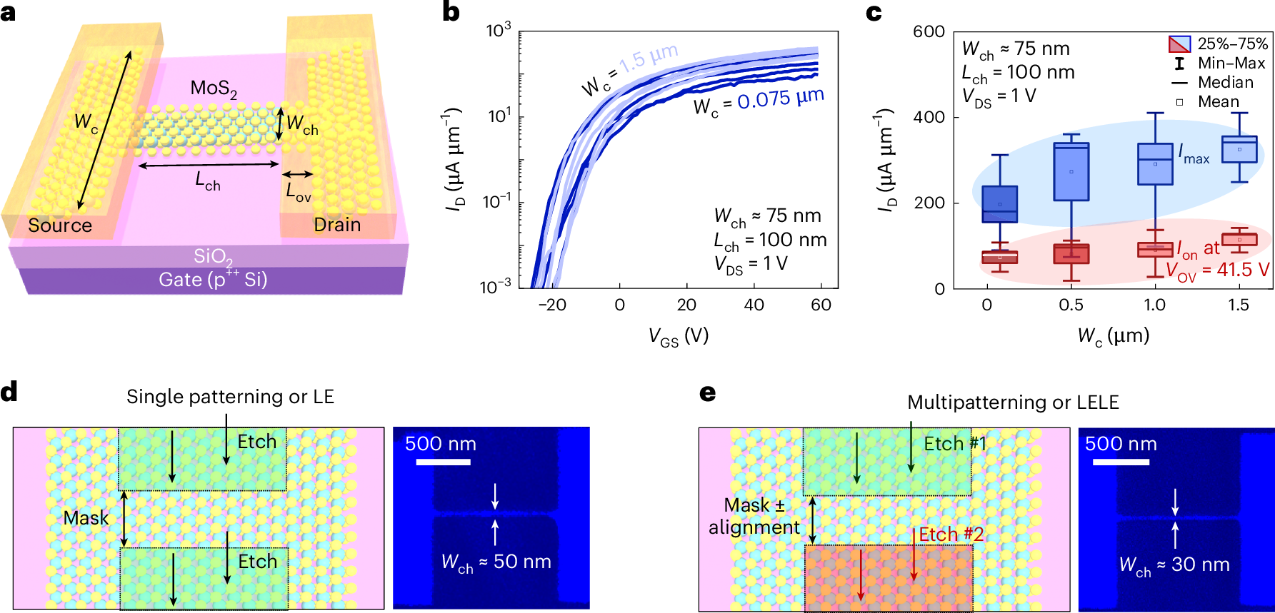
Nanoscale transistors demand aggressive scaling of all channel dimensions—length, width and thickness. Two-dimensional semiconductors (2DS) provide the ultimate thickness limit, yet good device performance has largely remained restricted to micrometre-wide channels. Here we report monolayer 2DS nanoribbon transistors with both n- and p-type operation, fabricated by a top-down multipatterning process that includes ‘anchored’ contacts to limit nanoribbon delamination. This approach achieves channel lengths and widths down to 25–30 nm, with minimal edge degradation confirmed through nanoscale characterization, including tip-enhanced photoluminescence. Integrated with thin high-κ gate dielectrics, the devices deliver on-state currents up to 560, 420 and 130 µA µm−1 at a drain-to-source voltage of 1 V for n-type MoS2, n-type WS2 and p-type WSe2, respectively. These results exceed prior single-gated 2DS nanoribbon reports, with WS2 improving by more than two orders of magnitude, even for normally off (enhancement-mode) operation. Overall, these findings position top-down patterned 2DS nanoribbons as promising building blocks for future nanosheet transistor architectures.