2026-09-10 サンディア国立研究所(SNL)
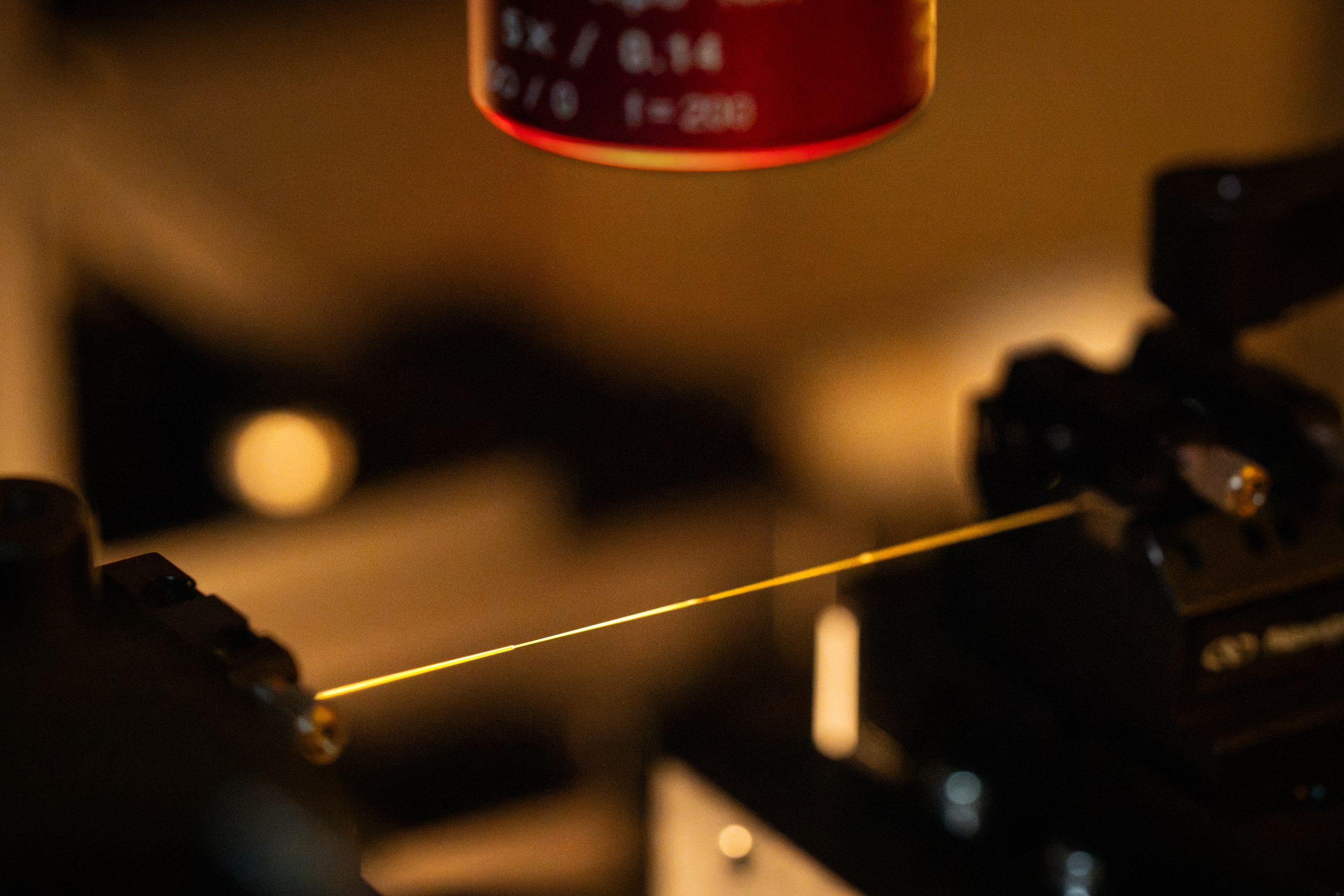
At Sandia National Laboratories, standard optical fiber is simultaneously heated over a flame and stretched by two motorized stages to produce an optical nanofiber.
<関連情報>
- https://newsreleases.sandia.gov/tight-light-helps-quantum-sensing-get-ready-for-the-field/
- https://pubs.aip.org/avs/aqs/article/8/3/033202/3398653/Optical-nanofiber-testbeds-for-benchmarking
オンチップ量子慣性センシングに向けた膜導波路フォトニック集積回路プラットフォームのベンチマーク評価のための光ナノファイバー試験台
Optical nanofiber testbeds for benchmarking membrane-waveguide photonic integrated circuit platforms toward on-chip quantum inertial sensing
Adrian Orozco;William Kindel;Nicholas Karl;Yuan-Yu Jau;Michael Gehl;Grant Biedermann;Jongmin Lee
AVS Quantum Science Published:July 16 2026
DOI:https://doi.org/10.1116/5.0309355
Recent advances in cold atom interferometry with optical and magnetic atom guides have set the stage for quantum inertial sensors capable of operating in dynamic environments. In this work, we present three key innovations—evanescent-field (EF) atom guides, optical nanofiber testbeds, and membrane-waveguide photonic integrated circuit (PIC) platforms—to advance EF-guided atom interferometry. First, we demonstrate EF atom guides on optical nanofiber testbeds, which serve as performance benchmarks for our membrane-waveguide PIC platforms. Second, we achieve low-power ( 5 mW) guiding of freely moving, laser-cooled 133Cs atoms in two-color, traveling-wave EF optical dipole traps at the novel, heat-efficient magic wavelengths of 793 and 937 nm (i.e., “793/937-nm EF atom guides”). Concurrently, we design and fabricate membrane-waveguide PIC platforms for these EF atom guides; in our prior work, we showed that these structures safely accommodate 4–6 times the required optical trap power under vacuum and enable dense cold atom generation via magneto-optical trapping in the vicinity of the optical wavguide for efficient loading. Third, we verify preserved atomic coherence via microwave fields and EF-coupled Doppler-free Raman beams; to our knowledge, this is the first report of coherence fringes driven by co-propagating EF-coupled Raman beams with only 150 nW of total optical power. By providing a direct comparison between optical nanofiber testbeds and membrane-waveguide PIC platforms, our results lay critical groundwork for the on-chip realization of EF-guided atom interferometry and the development of fully integrated, compact, lightweight, and low-power quantum accelerometers and gyroscopes.