2026-08-28 中国科学院(CAS)
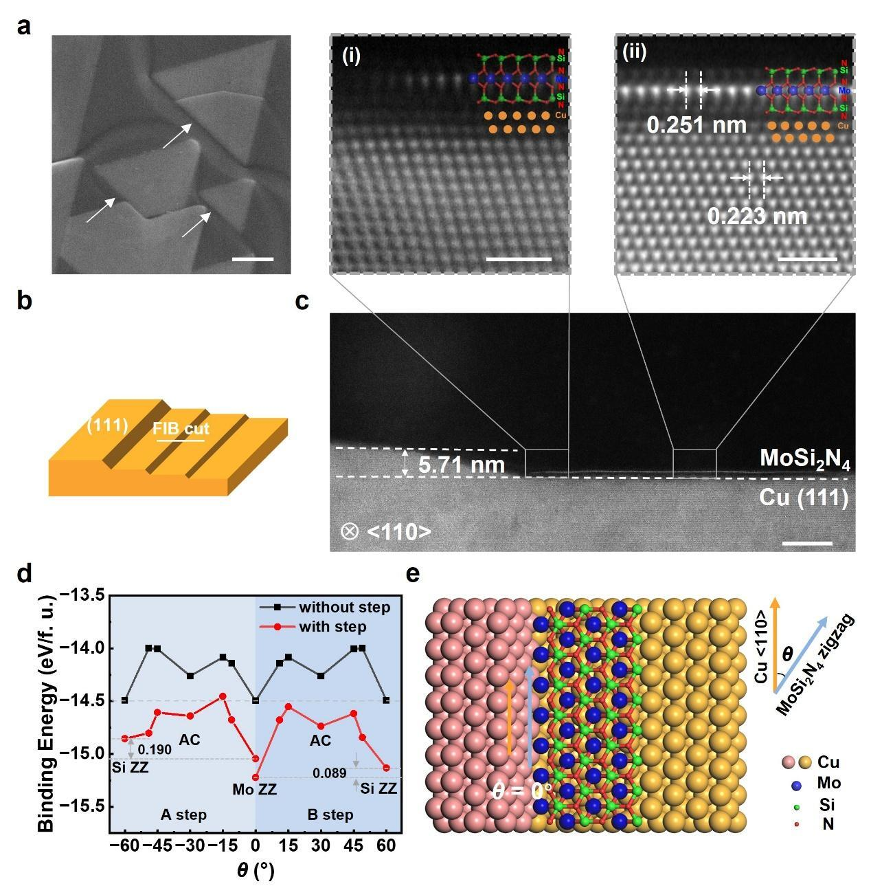
Single-orientation nucleation mechanism of monolayer MoSi2N4 induced by surface steps on Cu(111) single crystals. (Image by IMR)
<関連情報>
- https://english.cas.cn/newsroom/research-news/202608/t20260828_1189418.shtml
- https://www.nature.com/articles/s41563-026-02669-5
高安定性p型半導体単層MoSi₂N₄単結晶のウェハスケール成長 Wafer-scale growth of highly stable p-type semiconducting monolayer MoSi2N4 single crystals
Su Sun,Chuan Xu,Keqiang Ji,Yuexing Xia,Bo Tong,Jinmeng Tong,Chen Chen,Wenqin Zhao,Duanliang Zhou,Qinghe Wang,Lixin Yang,Qiang Wang,Miaomiao Li,Biyuan Zheng,Lai-Peng Ma,Xinfeng Liu,Zhibo Liu,Mengjian Zhu,Kaihui Liu,Peng Liu,Kaili Jiang,Hui-Ming Cheng & Wencai Ren
Nature Materials Published:08 July 2026
DOI:https://doi.org/10.1038/s41563-026-02669-5
Abstract
Single-crystal wafers of p-type two-dimensional (2D) semiconductors are highly desired for next-generation electronics. However, p-type 2D semiconductors remain scarce, and achieving wafer-scale monolayer single crystals of such materials is even more challenging. Here we report the wafer-scale growth of p-type semiconducting monolayer MoSi2N4 single crystals on Cu (111) foils with prestored Mo and Si atoms. The <110> steps on Cu (111) guide the nucleation and unidirectional orientation of monolayer MoSi2N4 domains, enabling their seamless stitching into a continuous single-crystal film. The resulting MoSi2N4 exhibits exceptional quality, with an intrinsic mobility of 154 cm2 V−1 s−1. Field-effect transistor arrays fabricated from this material deliver excellent electrical performance, including an on/off ratio of ~3.8 ± 1.4 × 10⁶ and an on-state current density up to ~17.96 μA μm−1 (1 μm channel length), along with superior stability compared with monolayer WSe2-based counterparts. Furthermore, this versatile growth strategy also enables the fabrication of wafer-scale monolayer WSi2N4 single crystals. This work establishes a promising p-type 2D semiconductor platform for future integrated circuits.