2026-09-03 ハーバード大学
<関連情報>
- https://seas.harvard.edu/news/new-device-design-could-miniaturize-photonics-quantum-technologies
- https://www.nature.com/articles/s41565-026-02268-0
自由空間アクセス可能な非線形分極増強のための量子井戸メタサーフェス Quantum-well metasurface for free-space-accessible enhanced nonlinear polarization
Pernille Undrum Fathi,Irene Occhiodori,Patrick Devaney,Amberly Ricks,Rithvik Ramesh,Yiwei Ju,Moaz Waqar,Theodore P. Letsou,Christina M. Spägele,Hyunseung Jung,Igal Brener,Xiaoqing Pan,Marcus Ossiander,Seth R. Bank & Federico Capasso
Nature Nanotechnology Published:02 September 2026
DOI:https://doi.org/10.1038/s41565-026-02268-0
Abstract
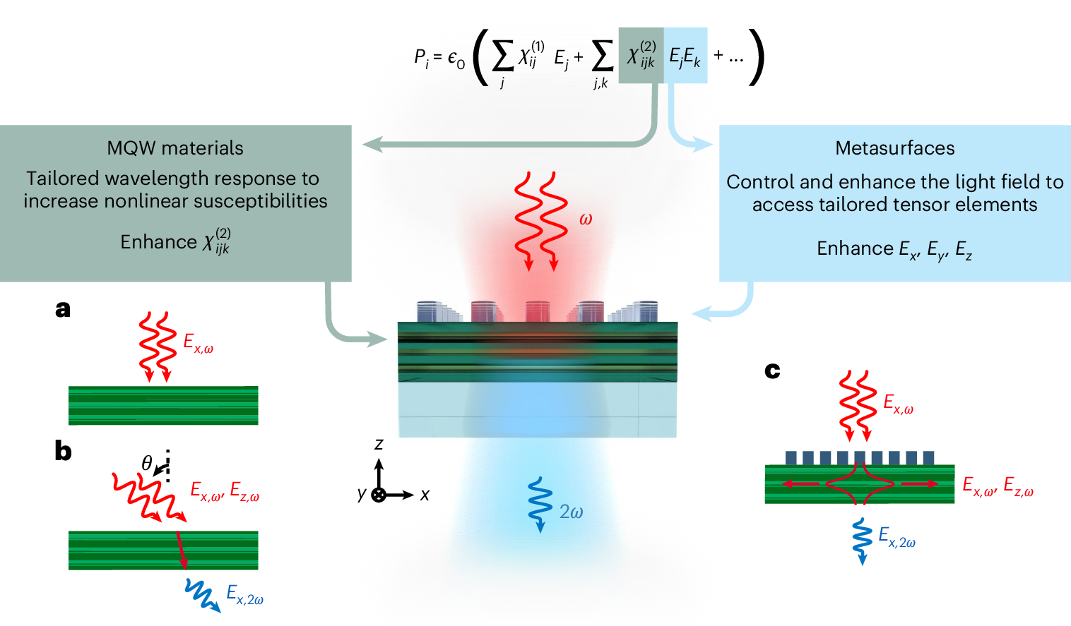
Nonlinear frequency conversion underpins important technologies such as telecommunications and quantum computation; however, weak nonlinearities and architectures that resist miniaturization currently limit devices’ efficiency and widespread adoption. Here we combine a band-structure-engineered GaAs/AlGaAs multi-quantum-well heterostructure with a high-quality-factor dielectric metasurface and symmetry-broken guided-mode field profiles to enhance the material nonlinear susceptibility. By engineering a resonant interband transition in the heterostructure, we realize a second-order nonlinear tensor element of 1.6 nm V−1 at 1.57 μm wavelength. We then make it free-space accessible and boost the effective nonlinearity to ~14 nm V−1 using a metasurface patterned on the material. Our proof-of-concept experiment establishes that combining interband-transition engineering and metasurfaces enables giant effective nonlinearities in the near-infrared to visible spectrum. This addresses material and device-level constraints in nonlinear photonics, providing a scalable route to compact, efficient devices.