2026-05-25 東京大学
東京大学と三菱ケミカルの研究グループは、耐圧kV級のGaN光伝導型スイッチ(PCSS)の動作実証に成功した。成果はISPSD 2026で発表予定である。研究では、Mn添加半絶縁性GaNバルク基板にSiイオン注入を施し、局所的なn型領域とオーミック接触を形成した構造を採用した。紫外光照射により明瞭な光電流が得られ、光キャリアのドリフト輸送によって動作することを確認した。さらに、Fe/C共添加GaN基板を用いた素子と比較して約40倍大きな光電流を達成し、Mn添加GaNの優位性を示した。オフ時には低リーク電流を維持し、最大2.4kVの耐圧を実証した。GaN PCSSは電気的ゲートを必要としないため、本質的に電磁干渉(EMI)が少なく、高速・高耐圧スイッチングが可能である。成果は、風力発電やメガソーラーなど再生可能エネルギー向け高効率電力変換技術への応用が期待される。今後はオン電流増大や表面構造最適化によるさらなる高耐圧化、高速スイッチング特性向上を目指す。

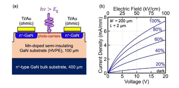
図1:(a) 本研究で作製したGaN PCSSの断面図(左図)。(b) GaN PCSSの光電流の電圧依存性及び光強度依存性(右図)。
<関連情報>
- https://www.t.u-tokyo.ac.jp/press/pr2026-05-25-001
- https://ieeexplore.ieee.org/abstract/document/11553953
Mnドープ半絶縁性GaNバルク結晶を用いたkV級GaN光伝導性半導体スイッチ kV-Class GaN Photoconductive Semiconductor Switches Using Mn-Doped Semi-Insulating GaN Bulk Crystals
Takuya Maeda, Chinwei Li, Ryosho Nakane, Kenji Iso
The 38th International Symposium on Power Semiconductor Devices and ICs (ISPSD 2026) Date Added to IEEE Xplore:11 June 2026
DOI:https://doi.org/10.1109/ISPSD64561.2026.11553953
Abstract
Photoconductive semiconductor switches (PCSSs) were fabricated using Mn-doped semi-insulating GaN substrates. The n+-GaN regions were selectively formed via Si-ion implantation followed by activation annealing, and Ti/Au was deposited as ohmic contacts. Current-voltage (I-V) characteristics of the GaN PCSSs were measured. Under monochromatic ultraviolet illumination (λ = 365 nm), a distinct photocurrent was observed that increased proportionally to optical power. Notably, the photocurrent was approximately 40 times larger than that of the Fe/C co-doped GaN PCSSs, reflecting the difference of carrier lifetimes. Under dark conditions, kV-class high breakdown voltages were demonstrated alongside low leakage current. These results showcase the significant potential of Mn-doped GaN PCSSs for high-power and high-speed power electronics applications free from electromagnetic interference (EMI).