(New Argonne etching technique could advance the way semiconductor devices are made)
2020-02-12 アメリカ合衆国・アルゴンヌ国立研究所(ANL)

・ ANL が、より微細で複雑な構造のデバイスの製造を可能にする、分子層エッチング(molecular layer etching: MLE)技術を開発。
・ 半導体デバイスのようなマイクロエレクトロニクスは、日常的な技術の核心をなすもの。「ムーアの法則」の限界が迫る時代への移行において、個別のデバイスにより多くの回路を詰め込む方法が必要となっている。
・ 現在は薄膜を層毎に積層・エッチングする技術を使用し、より微細なマイクロエレクトロニクスを製造している。薄膜を積層する分子層堆積(molecular layer deposition: MLD)技術と共に、MLE 技術はより微細なデバイス構造の設計に利用できる。
・ MLE・MLD の両技術は、マイクロエレクトロニクスの製造で一般的に利用される原子層堆積(atomic layer deposition: ALD)技術と原子層エッチング(atomic layer etchning: ALE)技術に類似したものだが、 ALD・ALE の両技術で扱えるのは無機材料膜のみ。MLD・MLE 技術は、有機材料膜の成長・除去に使用できる。
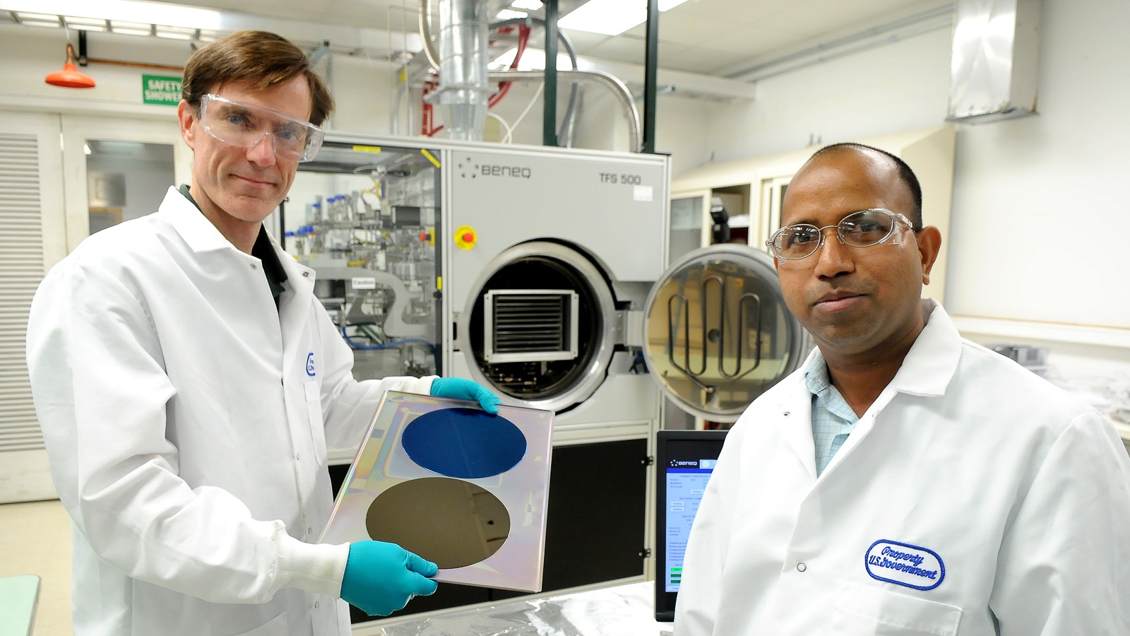
・ MLE 技術は、真空チャンバー内において数ナノ・マイクロメートルの薄さの膜にガスを導入するプロセス。最初にガス A に反応した薄膜表面を、次のガス B に露呈させる AB プロセスを繰り返すことで薄膜層を除去し、目的の薄さの膜を製造する。
・ このような AB 薄膜表面反応は、対象部位が無くなると自然に反応を停止する自己制御性。このことは、より大きな基板に向けてプロセスのスケールアップを比較的容易にするため、デバイス製造に極めて有利。
・ フレキシブルエレクトロニクスのアプリケーションの可能性が期待されるシリコーンゴムに類似した有機材料のアルコン(alcone)薄膜で、ガス A にはリチウム有機塩(LOS)、ガス B にはトリメチルアルミニウム(TMA)を使用し、同技術の実証試験を実施。
・ まず、リチウム化合物のリチウムがアルコン薄膜表面に付着して化学結合を阻害する反応を起こし、次に TMA によりリチウムを含有した層を除去する反応を確認。リチウムは、化学結合を断ちきるために暫定的に積層されて TMA により除去される犠牲層の役割を担った。層毎のプロセスを繰り返せば、最終的に全薄膜を除去することもできる。
・ 同技術は、製造業者や研究者にナノ構造を作る新方法を提供するもの。エッチングプロセスでは一般的な強力な化学物質のハロゲンを使用しないため、ナノ構造をより安全に製造できる。また、近接する ALD 層に影響を与えずに MLD 層を選択的に除去することも可能。
・ 本研究には、米国エネルギー省(DOE)の科学局が支援する Energy Frontier Research Center である、Center for Electrochemical Energy Science が資金を提供した。
URL: https://www.anl.gov/article/new-argonne-etching-technique-could-advance-the-waysemiconductor-devices-are-made
(関連情報)
Chemistry Materials 掲載論文(アブストラクトのみ:全文は有料)
Molecular Layer Etching of Metalcone Films Using Lithium Organic Salts and Trimethylaluminum
URL: https://pubs.acs.org/doi/10.1021/acs.chemmater.9b03627#
<NEDO海外技術情報より>
Abstract
Advances in semiconductor device manufacturing are limited by our ability to precisely add and remove thin layers of material in multistep fabrication processes. Recent reports on atomic layer etching (ALE) have provided the means for the precise removal of inorganic thin films deposited by atomic layer deposition (ALD), opening new avenues for nanoscale device design. Here, we report on a new technique for the precise removal of metal–organic thin films deposited by molecular layer deposition (MLD), which we term molecular layer etching. This etching process employs sequential exposures of lithium organic salt (LOS) and trimethylaluminum (TMA) precursors to produce self-limiting etching behavior. We employ quartz crystal microbalance experiments to demonstrate (i) etching of alucone films preloaded with LOS upon TMA exposures and (ii) layer-by-layer etching of alucone films using alternating exposures of LOS and TMA. We also identify the selectivity of these etching mechanisms. We probe the mechanism for the layer-by-layer etching of alucone using a quartz crystal microbalance and Fourier transform infrared spectroscopy and identify that the etching proceeds via heterolytic cleaving of Al–O bonds in alucone upon LOS exposure followed by methylation to produce volatile species upon TMA exposure. The etching process results in the removal of 0.4 nm/cycle of alucone at 160 °C and up to 3.6 nm/cycle of alucone at 266 °C in ex situ etching experiments on silicon wafers. This halogen-free etching process enables etching of MLD films and provides new fabrication pathways for the control of material geometries at the nanoscale.

