2023-11-29 ワシントン大学セントルイス校
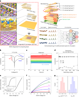
◆6つの原子薄い2Dレイヤーを密に組み合わせ、異なる機能を持たせることで、これまでのチップよりも優れた性能を実現しています。この技術は、電子およびコンピューティング業界を変革し、コンパクトで強力かつエネルギー効率の高いデバイスの開発を促進する可能性があります。
<関連情報>
- https://source.wustl.edu/2023/11/2d-material-reshapes-3d-electronics-for-ai-hardware/
- https://www.nature.com/articles/s41563-023-01704-z
究極のエッジコンピューティング・ソリューションに向けた2D材料ベースのエレクトロニクスのモノリシック3D統合 Monolithic 3D integration of 2D materials-based electronics towards ultimate edge computing solutions
Ji-Hoon Kang,Heechang Shin,Ki Seok Kim,Min-Kyu Song,Doyoon Lee,Yuan Meng,Chanyeol Choi,Jun Min Suh,Beom Jin Kim,Hyunseok Kim,Anh Tuan Hoang,Bo-In Park,Guanyu Zhou,Suresh Sundaram,Phuong Vuong,Jiho Shin,Jinyeong Choe,Zhihao Xu,Rehan Younas,Justin S. Kim,Sangmoon Han,Sangho Lee,Sun Ok Kim,Beomseok Kang,Seungju Seo,Hyojung Ahn,Seunghwan Seo,Kate Reidy,Eugene Park,Sungchul Mun,Min-Chul Park,Suyoun Lee,Hyung-Jun Kim,Hyun S. Kum,Peng Lin,Christopher Hinkle,Abdallah Ougazzaden,Jong-Hyun Ahn,Jeehwan Kim & Sang-Hoon Bae
Nature Materials Published:27 November 2023
DOI:https://doi.org/10.1038/s41563-023-01704-z

Abstract
Three-dimensional (3D) hetero-integration technology is poised to revolutionize the field of electronics by stacking functional layers vertically, thereby creating novel 3D circuity architectures with high integration density and unparalleled multifunctionality. However, the conventional 3D integration technique involves complex wafer processing and intricate interlayer wiring. Here we demonstrate monolithic 3D integration of two-dimensional, material-based artificial intelligence (AI)-processing hardware with ultimate integrability and multifunctionality. A total of six layers of transistor and memristor arrays were vertically integrated into a 3D nanosystem to perform AI tasks, by peeling and stacking of AI processing layers made from bottom-up synthesized two-dimensional materials. This fully monolithic-3D-integrated AI system substantially reduces processing time, voltage drops, latency and footprint due to its densely packed AI processing layers with dense interlayer connectivity. The successful demonstration of this monolithic-3D-integrated AI system will not only provide a material-level solution for hetero-integration of electronics, but also pave the way for unprecedented multifunctional computing hardware with ultimate parallelism.


