
2026-06-08 量子科学技術研究開発機,兵庫県立大学,高輝度光科学研究センター
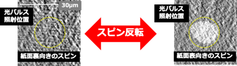
図1.作製した材料において光照射によって電子スピンの向きが反転する様子
<関連情報>
- https://www.qst.go.jp/site/press/20260608.html
- https://pubs.aip.org/aip/apl/article-abstract/128/23/232402/3394096/All-optical-switching-in-CoFeB-based-artificial
CoFeB系人工フェリ磁性体における全光スイッチング
All-optical switching in CoFeB-based artificial ferrimagnets
S. Li ;T. Ueno;R. Takahashi;H. Wadati;M. Ono;M. Notomi;Y. Ohtsubo;Y. Kotani;P. D. Bentley;S. Sakai
Applied Physics Letters Published:June 08 2026
DOI:https://doi.org/10.1063/5.0328535
We demonstrate deterministic all-optical switching (AOS) triggered by single femtosecond laser pulses in CoFeB-based artificial ferrimagnets consisting of Co/Gd/CoFeB trilayers. We show that AOS in this trilayer system is primarily governed by the energetics of nonequilibrium demagnetization, rather than by the magnetic anisotropy barrier in equilibrium. Unlike existing AOS multilayer systems in which CoFeB layers are coupled indirectly through a nonmagnetic layer, each layer in our system, including the CoFeB layer, is directly antiferromagnetically exchange-coupled by a strong interfacial proximity effect. This direct coupling enables a purely thermal toggle switching process across the entire stack, facilitating ultrafast optical writing. Moreover, these thin film structures are fully compatible with the high-magnetoresistance CoFeB/MgO/CoFeB tunnel junction architecture, making this system a promising building block for the development of all-optically driven magnetic tunnel junctions, which are a key component for future high-speed, low-power logic and memory applications.

