2026-07-27 分子科学研究所

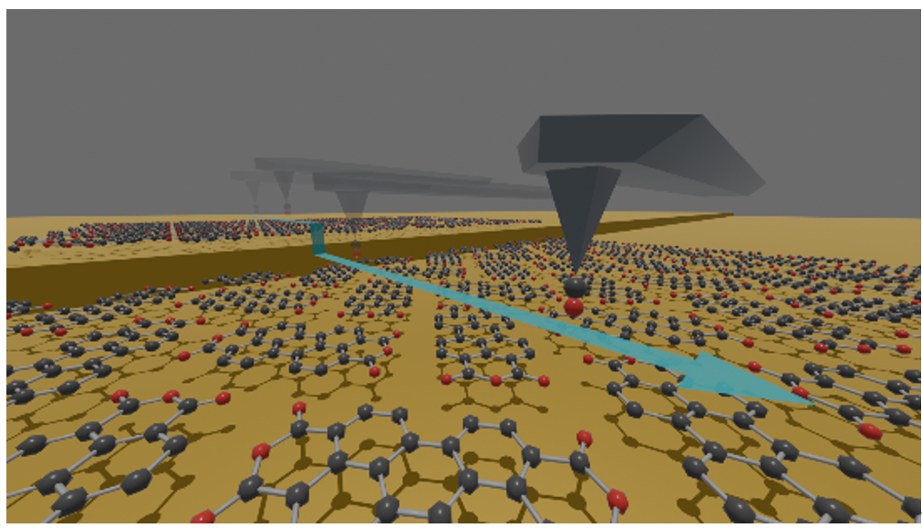
図1原子ホログラフィー顕微鏡の概念図
<関連情報>
- https://www.ims.ac.jp/news/2026/07/0727.html
- https://pubs.aip.org/aip/rsi/article-abstract/97/7/073702/3399228/Realizing-an-atom-holography-microscope
原子ホログラフィー顕微鏡の実現
Realizing an atom-holography microscope
Hiroshi Daimon;Hiroki Momono;Hiroyuki Matsuda;Fumihiko Matsui;Akiko Kubota;Kaho Hirano;Shinako Iki;Yu Masuda;Koichi Moriguchi;Keiko Ogai;Yusuke Hashimoto;Tomohiro Matsushita
Review of Scientific Instruments Published:July 24 2026
DOI:https://doi.org/10.1063/5.0331644
The precise determination of three-dimensional (3D) atomic coordinates is the cornerstone of materials analysis, but conventional transmission electron microscopy is limited to visualizing only two-dimensional projections. The direct observation of the true 3D atomic arrangement has, therefore, remained an elusive goal in materials science. Atomic-resolution holography is a powerful technique capable of analyzing the 3D atomic arrangement, even around isolated atoms. However, it typically requires allocated time at large-scale synchrotron radiation facilities, which has hindered its widespread adoption and integration into routine materials characterization workflows. Here, we show the realization of an atom-holography microscope that breaks this fundamental constraint, enabling atomic-resolution holography to be performed anytime and anywhere. Our novel microscope integrates a hologram-display electron spectrometer and a Scanning Electron Microscope (SEM), allowing for the visualization of the 3D atomic arrangement within a microscopic region in a SEM image. As a proof of concept, we analyzed a Kikuchi electron hologram obtained from a Bi2Se3 sample and successfully reconstructed the atomic arrangement with an accuracy of 0.1 Å. This result demonstrates that advanced analytical microscope capable of mapping the composition and 3D atomic arrangement of each pixel in a SEM image is now available anytime, anywhere, which is expected to significantly accelerate the development of highly functional materials and microdevices.