
2026-07-24 ハーバード大学
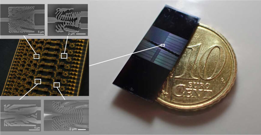
A photonic microchip, next to a 10-euro-cent coin for scale, containing hundreds of inverse-designed components. The close-up images show computer-designed nanostructures, wavelength splitters, mode sorters, and mirrors. The left illustration shows how such devices could be combined and densely packed into integrated photonic circuits on a chip. Credit: Tony Bi / MPL
<関連情報>
- https://seas.harvard.edu/news/algorithm-designed-photonic-circuits-beyond-human-intuition-0
- https://www.nature.com/articles/s41467-026-73390-9
逆設計型窒化ケイ素ナノフォトニクス Inverse-designed silicon nitride nanophotonics
Toby Bi,Shuangyou Zhang,Egemen Bostan,Danxian Liu,Aditya Paul,Olga Ohletz,Irina Harder,Yaojing Zhang,Alekhya Ghosh,Abdullah Alabbadi,Masoud Kheyri,Tianyi Zeng,Jesse Lu,Kiyoul Yang & Pascal Del’Haye
Nature Communications Published:28 May 2026
DOI:https://doi.org/10.1038/s41467-026-73390-9
Abstract
Silicon nitride photonics has enabled integration of a variety of components for applications in linear and nonlinear optics, including telecommunications, optical clocks, astrocombs, bio-sensing, and LiDAR. With the advent of inverse design – where desired device performance is specified and closely achieved through iterative, gradient-based optimisation – and the increasing availability of silicon nitride photonics via foundries, it is now feasible to expand the photonic design library beyond the limits of traditional approaches and unlock new functionalities. In this work, we present inverse-designed photonics on a silicon nitride platform and demonstrate both the design capabilities and experimental verification by realising precisely tailored wavelength-division multiplexers, mode-division multiplexers, and high-Q resonators with controllable wavelength range and dispersion. This demonstrates inverse-designed enhanced manipulation of orthogonal bases of light. Furthermore, we use these inverse-designed structures to form optical cavities that hold promise for on-chip nonlinear and quantum optics experiments.

