

2026-09-24 ロイヤルメルボルン工科大学(RMIT)
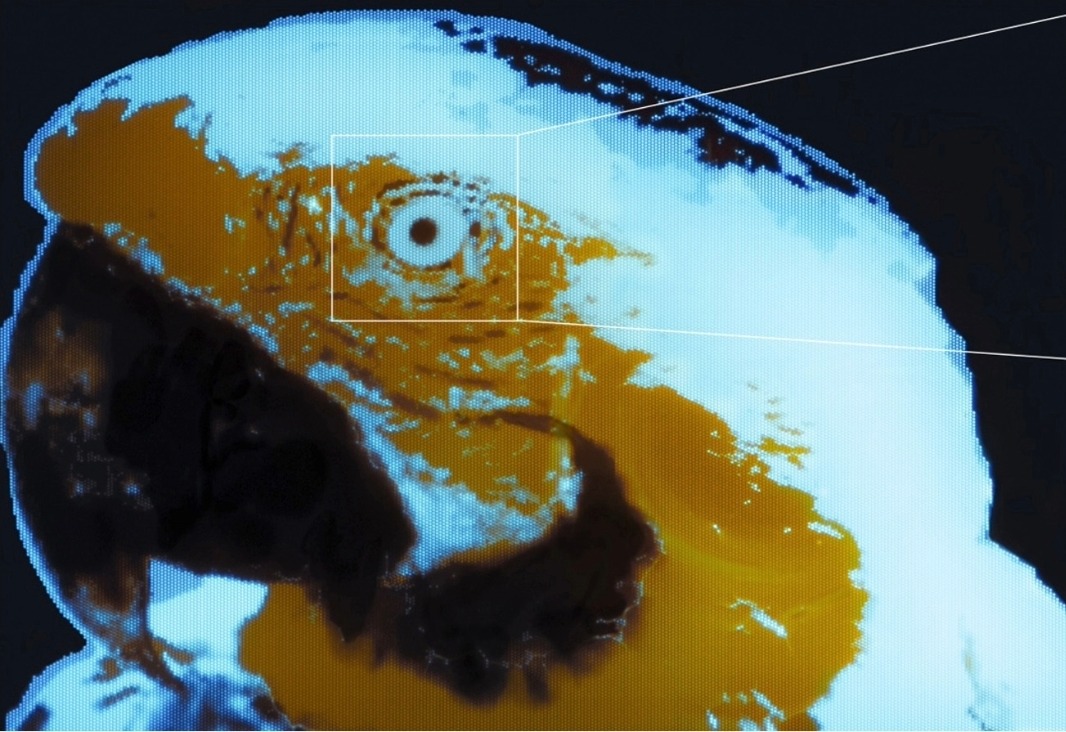
A record: the highest-resolution multicolour image using fluorescent dyes. Microscopic image. The image is 0.3 by 0.43 millimetres in size. Credit: Lo SW et al., Nature 2026.
<関連情報>
- https://www.rmit.edu.au/news/all-news/2026/sep/oleds
- https://www.nature.com/articles/s41586-026-11042-0
エレクトロルミネッセンスフォトレジストにより、リソグラフィのスケーリングをOLEDに拡張 Electroluminescent photoresists extending lithographic scaling to OLEDs
Shao-Wei Lo, Sunil B. Shivarudraiah, Zhan-Hong Lin, Patrick Helbling, Lifei Song, Jiachen Wang, Miguel Nouman, Fuze Jiang, Gerrit Stemmler, Donato Maria Carretta, Mei-Nung Chen, Jiayi Zhu, Sudhir Kumar, Hua Wang, Andrew J. Christofferson, Yinyin Bao & Chih-Jen Shih
Nature Published:16 September 2026
DOI:https://doi.org/10.1038/s41586-026-11042-0
Abstract
The miniaturization of organic light-emitting diodes is critical for next-generation ultrahigh-resolution displays and integrated photonics1,2,3,4,5,6,7,8. However, traditional vacuum evaporation and inkjet printing methods are incompatible with the lithographic scaling processes that underpin silicon electronics9,10,11,12,13,14,15,16, hindering true monolithic integration with complementary metal–oxide–semiconductor circuits. Here we present electroluminescent photoresists synthesized via atom transfer radical polymerization that can be directly patterned by ultraviolet and electron-beam lithography. These multi-arm star polymers feature a core–shell architecture designed to embed the thermally activated delayed fluorescence emitters within a protective host shell, segregating them from the reactive photocrosslinking moieties on the surface. The site-specific isolation ensures that crosslinking reactions occur at the periphery, leaving the emissive cores intact and preserving high electroluminescence. We demonstrate robust processing orthogonality in sequential multilayer electroluminescent photoresist photolithography, enabling subdiffraction fluorescence nanopatterns with critical dimensions down to 110 nm. We validate their device performance with multicolour, ultraviolet-patterned organic light-emitting diodes exhibiting external quantum efficiencies exceeding 13%. These results not only pave the way for extending Moore’s law to organic optoelectronics but also unlock their potential for monolithic optoelectronic integration.

