


2026-11-18 名古屋大学
<関連情報>
- https://www.nagoya-u.ac.jp/researchinfo/result/2026/11/20261118-engg.html
- https://onlinelibrary.wiley.com/doi/10.1002/smll.76581
凍結電気二重層を利用した単層発光デバイスへの超高電流注入
Frozen Electric Double Layers Enable Redox-Window-Unlimited Ultrahigh Current Injection in Monolayer Light-Emitting Devices
Koshi Oi, Hao Ou, Takahiko Endo, Jiang Pu, Yasumitsu Miyata, Akitoshi Nakano, Taishi Takenobu
Small(2026年11月17日オンライン公開)
DOI: https://doi.org/10.1002/smll.76581

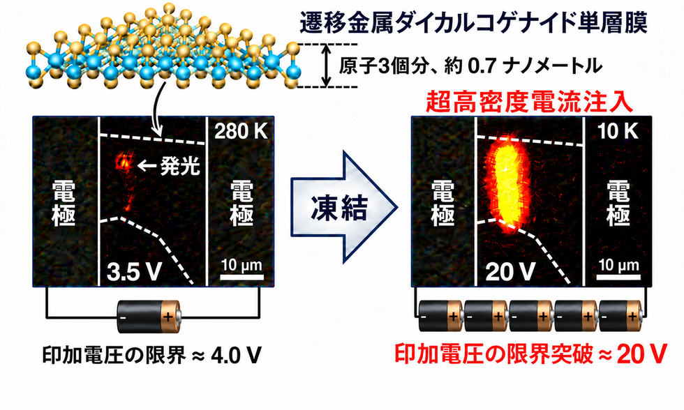
FIGURE 1 Schematic illustration of the frozen monolayer WSe2 electric-double-layer light-emitting device (EDLED) and its operating principle. Arrows between panels indicate the transition between the illustrated device states. (a) Schematic overview of the EDLED. The lower part shows the device structure, consisting of two-terminal electrodes on a substrate, a monolayer WSe2 bridging the electrodes, and an electrolyte layer formed on top. The upper left and upper right show a photograph of the ionic liquid at room temperature and the chemical structures of [DEME][TFSI] and PS–PMMA–PS, respectively. (b) Initial ionic migration immediately after bias application between the two-terminal electrodes. The arrows indicate the direction of ion motion under the applied electric field. (c) Formation of ionic sheets at the monolayer/electrolyte interface after sufficient time under an applied voltage. (d) Formation of electric double layers (EDLs) at the monolayer/electrolyte interface following electron and hole injection. (e) Lateral PN junction formation induced by EDLs, leading to electroluminescence. (f) Frozen state of the EDLED at low temperature, in which the ions are immobilized, and the pre-formed PN junction is preserved. (g) Frozen EDLED operated at a bias beyond the electrochemical stability (redox) window. © Oi et al., 2026. Licensed under Creative Commons Attribution License (CC BY).
3. English Summary
Electrolyte-gated transition metal dichalcogenide (TMDC) light-emitting devices can achieve high carrier densities, but their operating voltage is limited by the electrochemical stability window of the electrolyte. In this study, the researchers developed a strategy to overcome this limitation by forming a lateral PN junction in monolayer WSe₂ using electric double-layer doping and then cooling the device to 10 K under an applied bias to immobilize the ionic configuration. This preserves the junction while suppressing electrochemical reactions, enabling operation at voltages up to 20 V and a maximum current density of 0.8 MA cm⁻². Electroluminescence intensity increased with applied voltage, while the emission spectrum remained largely unchanged. This approach could provide a foundation for next-generation optoelectronic devices based on atomically thin semiconductors, including electrically driven high-density excitonic and polaritonic systems and laser-relevant devices.

