
2026-11-05 ワシントン大学セントルイス校
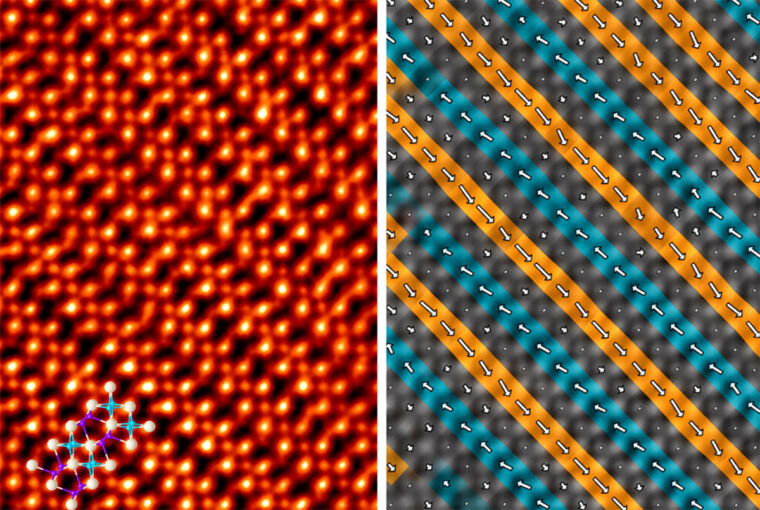
Atomic-resolution STEM image of La-doped HfO₂ (left) and the corresponding oxygen displacement vector map (right), revealing alternating antipolar layers with oppositely oriented local polarization, highlighted in orange and blue. (Image courtesy of Mishra lab)
<関連情報>
- https://source.washu.edu/2026/11/harnessing-atomic-structure-to-advance-semiconductor-technology/
- https://advanced.onlinelibrary.wiley.com/doi/10.1002/adma.75144
- https://www.science.org/doi/10.1126/science.ady5526
ZrO₂における帯電180°壁を介したサブnm2強誘電ドメイン Sub-nm2 Ferroelectric Domains via Charged 180° Walls in ZrO2
Nashrah Afroze, Hamoon Fahrvandi, Guodong Ren, Pawan Kumar, Christopher Nelson, Sarah Lombardo, Mengkun Tian, Ping-Che Lee, Jiayi Chen, Manifa Noor, Kisung Chae, Sanghyun Kang, …
Advanced Materials Published: 21 October 2026
DOI:https://doi.org/10.1002/adma.75144
Abstract
Flat phonon bands in fluorite ferroelectrics (HfO2 or ZrO2) shrink polar domains laterally to an irreducible half-unit-cell width (∼0.27 nm) within which the vertical arrangement of dipoles is expected to remain uniform. Here, we report on the direct observation of nonuniform and nearly discrete vertical arrangements of dipoles in ZrO2 thin films consisting of closely spaced head-to-head (HH) and tail-to-tail (TT) charged 180∘ walls, each exhibiting a distinct bulk-like structure. These charged domain walls (CDWs) further compress the irreducibly narrow, laterally stacked domains vertically to a thickness of ∼1–2.75 nm, yielding in-plane domains with sub-nm2 footprints—among the smallest ever reported for any ferroelectric material. The HH and TT walls form due to their flat longitudinal optical (LO) polar bands, and the former are electrostatically stabilized by bound-charge compensation via interstitial oxygen atoms, which act as natural structural defects at the HH walls. Moreover, these walls are predicted to be conducting and to exhibit ultralow propagation barriers, with HH walls (1.6 meV) being far more mobile than TT walls (22.3 meV), indicating strong potential for low-voltage, domain-wall-based nanoelectronics.
2次元限界までの反強誘電性ハフニア Antiferroelectric hafnia down to the 2D limit
Xin Li, Guodong Ren, Haidong Lu, Kartik Samanta, Amit Kumar Shah, Kai Huang, Pravan Omprakash, Yu Yun, Pratyush Buragohain, […] , and Xiaoshan Xu
Science Published:24 Sep 2026
DOI:https://doi.org/10.1126/science.ady5526
Abstract
Antiferroelectricity is a material property characterized by alternating electric dipoles spontaneously ordered in antiparallel directions. Antiferroelectrics are promising for energy storage, solid-state cooling, and memory technologies; however, these materials are scarce, and their scalability remains largely unexplored. In this work, we demonstrate that single-crystalline hafnia, a lead-free CMOS-compatible material, exhibits antiferroelectricity under compressive-strain conditions. We observe antiparallel sublattice polarization and stable double-hysteresis in single-crystalline (111)-oriented epitaxial La-doped hafnia films grown on yttrium-stabilized zirconia and show that the antipolar orthorhombic phase of hafnia adheres to the Kittel model of antiferroelectricity. Notably, compressive strain strengthens the orthorhombic order in thinner La-doped hafnia films, achieving a very high ordering temperature of 850°C in the two-dimensional limit, highlighting hafnia’s potential for advanced antiferroelectric devices.

