")
2024-01-18 ジョージア工科大学
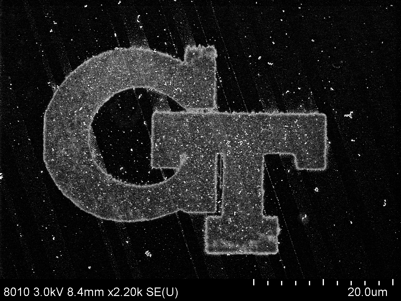
Scanning electron microscope image of a printed silver Georgia Tech logo made with the researchers’ SLP technique. Credit: Jungho Choi
◆スーパールミネッセント発光ダイオードを使用した低コストな光源を組み合わせ、プロジェクション型の印刷技術を構築。低コストで高速かつ鮮明な焦点を持つナノ構造の印刷が可能となりました。
<関連情報>
- https://research.gatech.edu/researchers-create-faster-and-cheaper-way-print-tiny-metal-structures-light
- https://onlinelibrary.wiley.com/doi/10.1002/adma.202308112
超光投影による金属ナノ構造のスケーラブルな印刷 Scalable Printing of Metal Nanostructures through Superluminescent Light Projection
Jungho Choi, Sourabh K. Saha
Advanced Materials Published: Published: 22 October 2023
DOI:https://doi.org/10.1002/adma.202308112
Abstract
Direct printing of metallic nanostructures is highly desirable but current techniques cannot achieve nanoscale resolutions or are too expensive and slow. Photoreduction of solvated metal ions into metallic nanoparticles is an attractive strategy because it is faster than deposition-based techniques. However, it is still limited by the resolution versus cost tradeoff because sub-diffraction printing of nanostructures requires high-intensity light from expensive femtosecond lasers. Here, this tradeoff is overcome by leveraging the spatial and temporal coherence properties of low-intensity diode-based superluminescent light. The superluminescent light projection (SLP) technique is presented to rapidly print sub-diffraction nanostructures, as small as 210 nm and at periods as small as 300 nm, with light that is a billion times less intense than femtosecond lasers. Printing of arbitrarily complex 2D nanostructured silver patterns over 30 µm × 80 µm areas in 500 ms time scales is demonstrated. The post-annealed nanostructures exhibit an electrical conductivity up to 1/12th that of bulk silver. SLP is up to 480 times faster and 35 times less expensive than printing with femtosecond lasers. Therefore, it transforms nanoscale metal printing into a scalable format, thereby significantly enhancing the transition of nano-enabled devices from research laboratories into real-world applications.
")
")