2022-09-06 ノースカロライナ州立大学(NCState)

2021年に発表された論文で、研究者達は、イオン注入と活性化を用いて、GaN材料に狙った領域をドープする技術を概説しています。つまり、GaN材料上の特定の領域に不純物を細工して、その領域だけGaNの電気特性を選択的に変化させた。
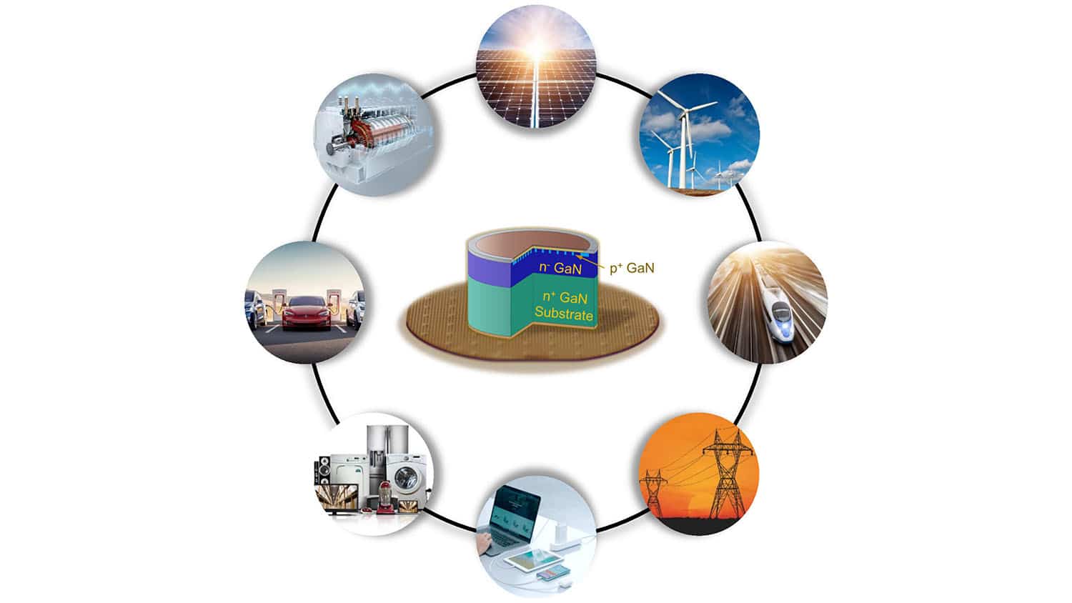
今回の論文では、この技術を実際のデバイスに応用できることを実証した。具体的には、選択的にドーピングされたGaN材料を用いて、JBS(Junction Barrier Schottky)ダイオードを作製した。
<関連情報>
- https://news.ncsu.edu/2022/09/new-gallium-nitride-devices/
- https://iopscience.iop.org/article/10.35848/1882-0786/ac8f81
超高圧アニールで活性化したMg注入による理想に近い性能を持つ縦型GaNジャンクションバリアショットキーダイオード Vertical GaN junction barrier Schottky diodes with near-ideal performance using Mg implantation activated by ultra-high-pressure annealing
Dolar Khachariya, Shane Stein, Will Mecouch, M. Hayden Breckenridge, Shashwat Rathkanthiwar, Seiji Mita, Baxter Moody, Pramod Reddy, James Tweedie, Ronny Kirste, Kacper Sierakowski, Grzegorz Kamler, Michal Bockowski, Erhard Kohn, Spyridon Pavlidis, Collazo Ramon and Zlatko Sitar
Applied Physics Express Accepted Manuscript online 5 September 2022
DOI: https://doi.org/10.35848/1882-0786/ac8f81
Abstract
We report a kV class, low ON-resistance, vertical GaN junction barrier Schottky (JBS) diode with selective-area p-regions formed via Mg implantation followed by high-temperature, ultra-high pressure (UHP) post-implantation activation anneal. The JBS has an ideality factor of 1.03, a turn-on voltage of 0.75 V, and a specific differential ON-resistance of 0.6 mΩ·cm2. The breakdown voltage of the JBS diode is 915 V, corresponding to a maximum electric field of 3.3 MV/cm. These results underline that high-performance GaN JBS can be realized using Mg implantation and high-temperature UHP post-activation anneal.
As the Version of Record of this article is going to be/has been published on a subscription basis, this Accepted Manuscript will be available for reuse under a CC BY-NC-ND 3.0 licence after a 12 month embargo period.
Although reasonable endeavours have been taken to obtain all necessary permissions from third parties to include their copyrighted content within this article, their full citation and copyright line may not be present in this Accepted Manuscript version. Before using any content from this article, please refer to the Version of Record on IOPscience once published for full citation and copyright details, as permission may be required. All third party content is fully copyright protected, unless specifically stated otherwise in the figure caption of the Version of Record.


