2026-09-04 京都大学
<関連情報>
- https://www.t.kyoto-u.ac.jp/ja/research/topics/20260904
- https://advanced.onlinelibrary.wiley.com/doi/10.1002/adfm.78177
チタン酸ストロンチウム内のねじり粒界による原子スケール・超高密度スキルミオン格子の創出 Ultrahigh-Density Atomic-Scale Polar Skyrmion Lattice in SrTiO3 via Twist Grain Boundary Engineering
Masaya Kono, Kohta Kasai, Yoshitaka Ikeda, Tao Xu, Susumu Minami, Takahiro Shimada
Advanced Functional Materials Published: 03 September 2026
DOI:https://doi.org/10.1002/adfm.78177
ABSTRACT
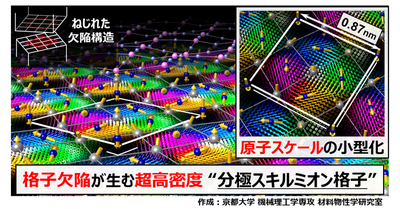
Skyrmions and nanoscale topologies in materials exhibit distinctive functionalities, including emergent electromagnetic fields, and offer promising applications, particularly as high-density information devices, owing to their lattice-forming nature. While reducing thickness according to Kittel’s law enables the miniaturization of polar topologies, an intrinsic size limit of 2 − 5 nm emerges in the ultrathin regime, precluding the realization of ultrasmall topologies in bulk materials suitable for practical applications. Here, we demonstrate that ultra-high-density lattices (1.32 nm−2) of atomic-scale polar skyrmions (0.87 nm), an order of magnitude smaller than existing polar skyrmions (and two orders smaller than magnetic skyrmions), emerge in SrTiO3 via twist grain boundary (GB) defect engineering. The stabilization of these polar skyrmions originates from the interfacial Coulomb interactions arising from the twisted atomic geometry. Owing to this mechanism, engineering the GB interface structures enables the spontaneous emergence of diverse topologies, including hybrid and antiferroelectric skyrmions, all at ultra-high densities. Moreover, these topological orders can be switched and transformed by applying external electric fields. This work suggests that defect engineering can complement Kittel’s law, enabling access to topology sizes and densities beyond those attainable through the conventional thickness-scaling approach.