2025-06-18 マサチューセッツ工科大学(MIT)

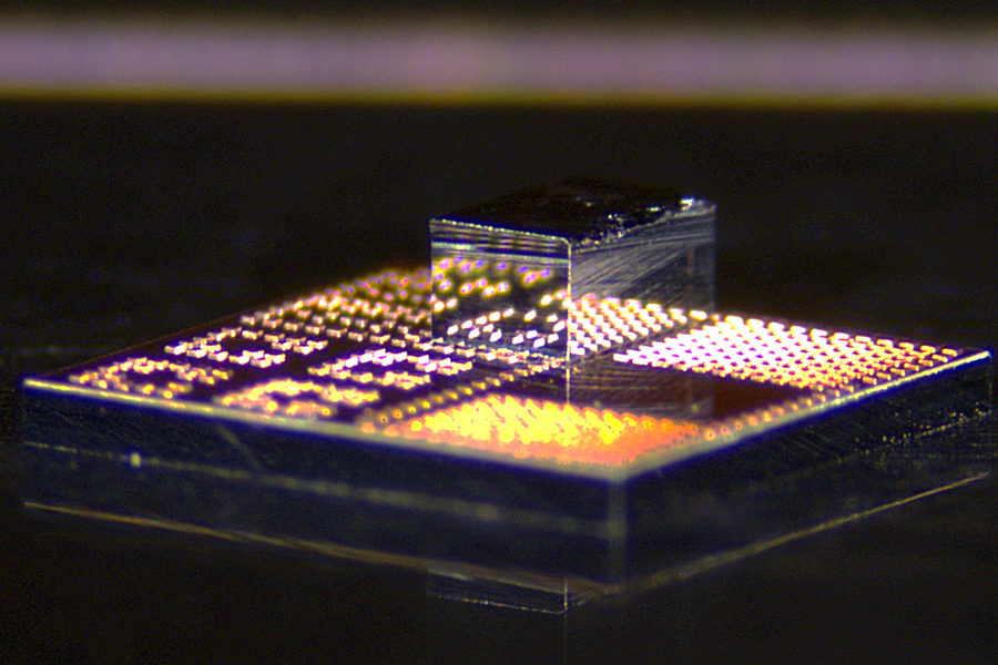
Researchers have developed a new fabrication process that integrates high-performance gallium nitride transistors onto standard silicon CMOS chips in a way that is low-cost and scalable. Credits:Image: Courtesy of the researchers
<関連情報>
- https://news.mit.edu/2025/new-3d-chips-could-make-electronics-faster-and-more-energy-efficient-0618
- https://rfic-ieee.org/technical-program/rfic-technical-sessions?date=2025-06-17
3次元ミリ波集積回路(3D-mmWIC): Intel 16 Si CMOSを用いたスケーリングRF GaN-on-Siダイレットのための金なし3D集積プラットフォーム 3D-Millimeter Wave Integrated Circuit (3D-mmWIC): A Gold-Free 3D-Integration Platform for Scaled RF GaN-on-Si Dielets with Intel 16 Si CMOS
Pradyot Yadav, Jinchen Wang, Danish A. Baig, Juan Pastrana-Gonzalez, John Niroula, Patrick Darmawi-Isakandar, Ulrich L. Rohde, Ahmad Islam, Muhannad Bakir, Ruonan Han, Tomás Palacios
IEEE Radio Frequency Integrated Circuits Symposium 15-17 June 2025 in San Francisco, CA
Abstract
This paper presents a gold-free 3D millimeter wave integrated circuit (3D-mmWIC). Highly scaled GaN-on-Si front-end-of-line (FEOL) RF dielets are integrated with Intel 16 Si CMOS using Cu-Cu thermocompression bonding (TCB), solder-free 3D heterogeneous integration (3DHI). To demonstrate this process, two different 3D-mmWIC amplifiers targeting the 5G NR FR2 band are fabricated utilizing multiple dielets. The first amplifier implements a conjugate matching of the dielets, achieving a maximum small-signal gain of 4.8 dB and a 3 dB bandwidth of 26–30 GHz. The second amplifier implements additional cross-neutralization capacitance to achieve a maximum small-signal gain of 6.2 dB and a 3 dB bandwidth of 26–32 GHz. Both 3D-mmWICs are extremely compact with a total chip area of 0.49 mm².


