2024-01-03 ジョージア工科大学
◆従来の電子機器の主成分であるシリコンが限界に達している中、新たな選択肢として使えるグラフェン半導体を生み出すことで、電子機器の進化が期待される。
◆研究者はグラフェンにバンドギャップを持たせ、シリコンの10倍の移動度を持つ優れた半導体を実現。これが実用化すれば、量子コンピューティングなど新たなテクノロジーへの道を開く可能性がある。
<関連情報>
- https://research.gatech.edu/feature/researchers-create-first-functional-semiconductor-made-graphene
- https://www.nature.com/articles/s41586-023-06811-0
炭化ケイ素上の超高移動度半導体エピタキシャルグラフェン Ultrahigh-mobility semiconducting epitaxial graphene on silicon carbide
Jian Zhao,Peixuan Ji,Yaqi Li,Rui Li,Kaimin Zhang,Hao Tian,Kaicheng Yu,Boyue Bian,Luzhen Hao,Xue Xiao,Will Griffin,Noel Dudeck,Ramiro Moro,Lei Ma & Walt A. de Heer
Nature Published:03 January 2024
DOI:https://doi.org/10.1038/s41586-023-06811-0

Abstract
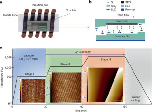
Semiconducting graphene plays an important part in graphene nanoelectronics because of the lack of an intrinsic bandgap in graphene1. In the past two decades, attempts to modify the bandgap either by quantum confinement or by chemical functionalization failed to produce viable semiconducting graphene. Here we demonstrate that semiconducting epigraphene (SEG) on single-crystal silicon carbide substrates has a band gap of 0.6 eV and room temperature mobilities exceeding 5,000 cm2 V−1 s−1, which is 10 times larger than that of silicon and 20 times larger than that of the other two-dimensional semiconductors. It is well known that when silicon evaporates from silicon carbide crystal surfaces, the carbon-rich surface crystallizes to produce graphene multilayers2. The first graphitic layer to form on the silicon-terminated face of SiC is an insulating epigraphene layer that is partially covalently bonded to the SiC surface3. Spectroscopic measurements of this buffer layer4 demonstrated semiconducting signatures4, but the mobilities of this layer were limited because of disorder5. Here we demonstrate a quasi-equilibrium annealing method that produces SEG (that is, a well-ordered buffer layer) on macroscopic atomically flat terraces. The SEG lattice is aligned with the SiC substrate. It is chemically, mechanically and thermally robust and can be patterned and seamlessly connected to semimetallic epigraphene using conventional semiconductor fabrication techniques. These essential properties make SEG suitable for nanoelectronics.


