2026-10-21 高エネルギー加速器研究機構,科学技術振興機構
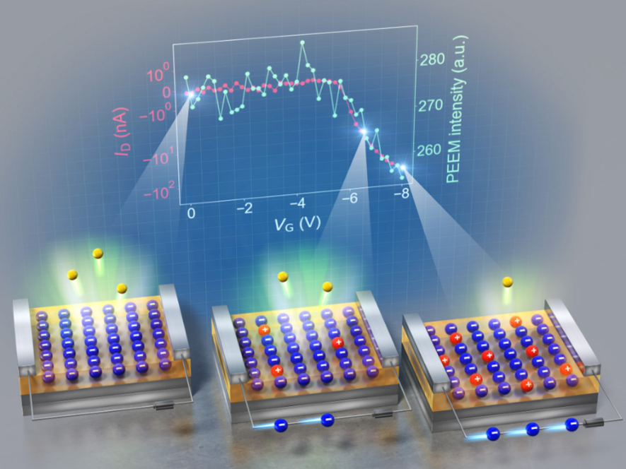
図1 半導体デバイスは、電子と正孔、または、どちらかが電荷キャリアとして動くことで機能している。本研究では、トランジスタが動作する環境下で正孔の可視化に成功。
<関連情報>
- https://www.kek.jp/ja/press/202610211400
- https://pubs.aip.org/aip/apr/article/13/4/041410/3406895/Imaging-conducting-holes-in-field-effect
電界効果トランジスタにおける伝導性ホールのイメージング
Imaging conducting holes in field-effect transistors
Keiki Fukumoto;Kosuke Yoshikawa;Konoha Shimizu;Elizaveta Pyatenko;Yoichi Yamada;Yutaka Wakayama;Ryoma Hayakawa
Applied Physics Review Published:October 21 2026
DOI:https://doi.org/10.1063/5.0335842
Holes and electrons are indispensable charge carriers in various electronic and optoelectronic devices. However, holes are quasiparticles described as the absence of electrons, and their signals are often buried under strong electron-derived signals, making observation challenging. In this study, we propose a highly sensitive imaging method based on photoemission electron microscopy with a photon-energy-tunable laser source to visualize hole accumulation at the organic semiconductor–insulator interface in an organic field-effect transistor. By tuning the photon energy of the excitation source to the energy level corresponding to the top of the highest occupied molecular orbital, hole accumulation in an organic semiconductor could be detected as a decrease in photoemission intensity under an applied gate voltage. The proposed method has the potential to unveil the carrier transport mechanism in a wide range of semiconductor-based devices with real-time imaging of hole transport and accumulation. It thus paves the way for the development of state-of-the-art electronic devices.