2026-07-16 アリゾナ大学
<関連情報>
- https://news.arizona.edu/news/quantum-materials-discovery-could-advance-electronics-extreme-environments
- https://pubs.acs.org/doi/10.1021/acsami.6c02516
9原子幅のアームチェア型グラフェンナノリボントランジスタのガンマ線照射に対する電気的および構造的応答 Electrical and Structural Response of Nine-Atom-Wide Armchair Graphene Nanoribbon Transistors to Gamma Irradiation
Kentaro Yumigeta,Muhammed Yusufoglu,John G. Federice,Elena T. Hughes,Ahmet Mert Degirmenci,Jon T. Njardarson,Kelly Simmons-Potter,Barrett G. Potter,and Zafer Mutlu
ACS Applied Materials & Interfaces Published: April 20, 2026
DOI:https://doi.org/10.1021/acsami.6c02516
Abstract
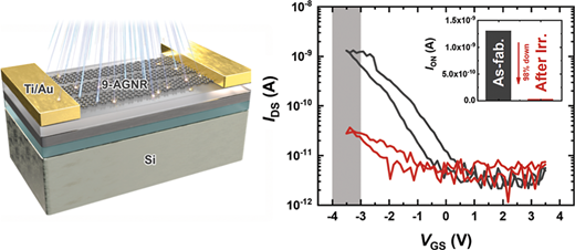
Materials and devices used in space and advanced energy systems are continuously exposed to high-energy photons and particles, leading to gradual changes in their structural and electronic properties. Gamma-ray exposure is particularly critical because their strong penetrating power allows them to traverse conventional shielding and device packaging. Real-time monitoring of exposure-induced changes in compact, chip-integrated devices remain limited despite the availability of external radiation detectors. Atomically precise graphene nanoribbons (GNRs) present an attractive platform for probing such effects due to their structural uniformity, tunable electronic properties, and exceptional sensitivity of charge transport to even subtle lattice modifications, a capability not yet demonstrated in other low-dimensional materials. Here, we investigate the structural and electronic response of atomically precise GNRs to gamma irradiation. Nine-atom-wide armchair GNRs (9-AGNRs) were synthesized via a bottom-up on-surface approach, integrated into field-effect transistors (FETs), and characterized before and after exposure using Raman spectroscopy and electrical transport measurements. Raman spectroscopy indicates preservation of the primary GNR lattice structure, accompanied by subtle spectral changes suggestive of irradiation-induced oxidation or local lattice perturbations. While these measurements do not indicate severe structural damage, electrical transport measurements reveal a pronounced degradation in device performance, demonstrating the strong susceptibility of GNR FETs to gamma irradiation. This pronounced response may be attributed to Anderson localization of charge carriers, potentially arising from enhanced quantum interference in atomically narrow, quasi-one-dimensional (1D) GNRs. These results suggest the potential of GNR-based nanoelectronic devices for sensing and monitoring under extreme operational conditions.