2026-09-14 ペンシルベニア州立大学(Penn State)
<関連情報>
- https://www.psu.edu/news/earth-and-mineral-sciences/story/improved-thin-film-harnesses-indoor-light-power-devices
- https://www.nature.com/articles/s41560-026-02101-x
- https://pubs.aip.org/aip/ape/article/4/3/036103/3400497/Boosting-indoor-perovskite-photovoltaic
- https://pubs.rsc.org/tc/article/12/21/7562/877570/Anti-solvent-engineering-enables-efficient-ambient
屋内太陽光発電装置の性能と安定性を測定するためのベストプラクティス Best practices for measuring the performance and stability of indoor photovoltaic devices
Abhisek Chakraborty,Giulia Lucarelli,Vaibhav Singh,Jie Xu,Zeynab Skafi,Diksha Thakur,Francesco Di Giacomo,Gyanendra Shankar,Emanuele Calabrò,Francesca De Rossi,Osbel Almora,Peyman Amiri,Shinji Aramaki,Diego Bagnis,Tomiki Bannai,Christoph J. Brabec,Daniele Braga,Gregory Burwell,Francesca Brunetti,Aldo Di Carlo,Matt Carnie,Luigi Angelo Castriotta,Sergio Castro-Hermosa,Manuela Ciocca,… Thomas M. Brown
Nature Energy Published:18 August 2026
DOI:https://doi.org/10.1038/s41560-026-02101-x
Abstract
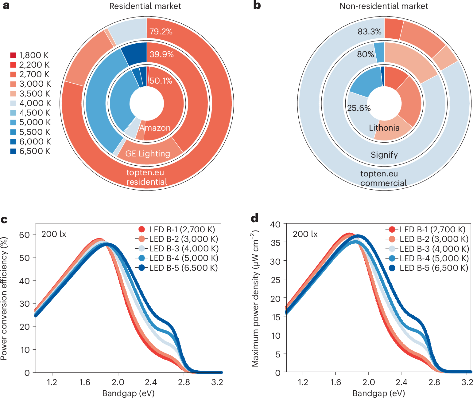
Indoor photovoltaics harvests energy from light available inside homes and buildings for powering the Internet of Things, wireless sensors and consumer and medical electronics. A major challenge in this field is a lack of standardized testing conditions. Here a team from more than 60 research institutions and companies proposes best practices for evaluating indoor photovoltaic performance and establishing baseline stability tests. We base these recommendations on recent experimental data, published literature, practices used in academic and industrial settings, technical specifications from standards organizations, lighting databases and existing regulations. We outline procedures that begin with the recommendation of a single artificial light source, followed by guidance on setting up measurement systems and a step-by-step guide for conducting measurements and tests. These procedures are consolidated into three checklists. Our aim is to promote accurate measurement of laboratory and commercial solar cells and modules under indoor lighting, facilitating comparability across academia and industry worldwide.
組成調整、溶媒エンジニアリング、および界面パッシベーションを統合することで、屋内ペロブスカイト太陽電池の性能を向上させる Boosting indoor perovskite photovoltaic performance via integrated compositional tuning, solvent engineering, and interfacial passivation
Justin Lin;Souk Y. Kim;Marvin H. Wu;Nutifafa Y. Doumon;Ivy M. Asuo
APL Energy Published:August 07 2026
DOI:https://doi.org/10.1063/5.0337271
Passivation of surface defects at the interface between perovskite absorber layers and charge transport layers is important for reducing ion migration and nonradiative recombination, thereby improving the performance of perovskite photovoltaics. In indoor photovoltaics, the bandgap of the perovskite absorber layer must be engineered to optimize device performance, typically through compositional tuning of the precursor materials. Passivation becomes even more relevant when light intensity levels are low, as fewer charge carriers are generated and recombination can be much more detrimental. Herein, we simultaneously apply composition and anti-solvent engineering, varying bromine content in the perovskite and using chlorobenzene or dichlorobenzene, with phenethylammonium salts as interfacial passivators to (i) increase the crystallinity and grain sizes of the perovskite absorber layer, (ii) form a quasi-2D/3D perovskite heterojunction to passivate surface defects, and (iii) demonstrate light-intensity-dependent stability behavior. The optimized perovskite indoor photovoltaic devices with an aperture area of 0.093 cm2, using dichlorobenzene as the anti-solvent and phenethylammonium bromide as the passivation salt, achieved an improved efficiency of 36.2% with a power output of 112.2 μW cm−2, a fill factor of 76.5%, an open-circuit voltage of 1.04 V, and a short-circuit current density of 141.28 μA cm−2 under 1000 lux.
非溶媒工学により、効率的な常温プロセス型ハロゲン化物ペロブスカイト太陽電池が実現 Anti-solvent engineering enables efficient ambient-processed halide perovskite solar cells
Ivy M. Asuo;Arezo Mahdavi Varposhti;Enrique D. Gomez;Nutifafa Y. Doumon
Journal of Materials Chemistry C Published:07 May 2024
DOI:https://doi.org/10.1039/d4tc01305k
Organic–inorganic metal halide perovskite thin film formation is one of the major challenges for solution-processed perovskite optoelectronic and photovoltaic devices, in particular, in ambient conditions due to their hygroscopic nature. Therefore, to improve the quality, optical properties, and performance of ambient processed metal halide perovskite thin films, it is necessary to have control over the fabrication process. We demonstrate how compositional and morphological control of ambient-processed perovskite films can be achieved using anti-solvents. We compare how exposing the film to anti-solvents, including dichlorobenzene, ethanol, and chlorobenzene, affects the crystallization and device performance of ambient-processed planar heterojunction perovskite solar cells. We also analyzed the charge carrier dynamics of the devices and found that including dichlorobenzene leads to reduced charge carrier recombination. The incorporation of dichlorobenzene results in densely packed grains without voids, leading to the best-performing device with a reproducible power conversion efficiency of ∼20%. These findings open the possibility of developing low-cost, highly reliable perovskite solar cells for commercial applications in the future.