

2026-09-10 京セラ株式会社,東北大学
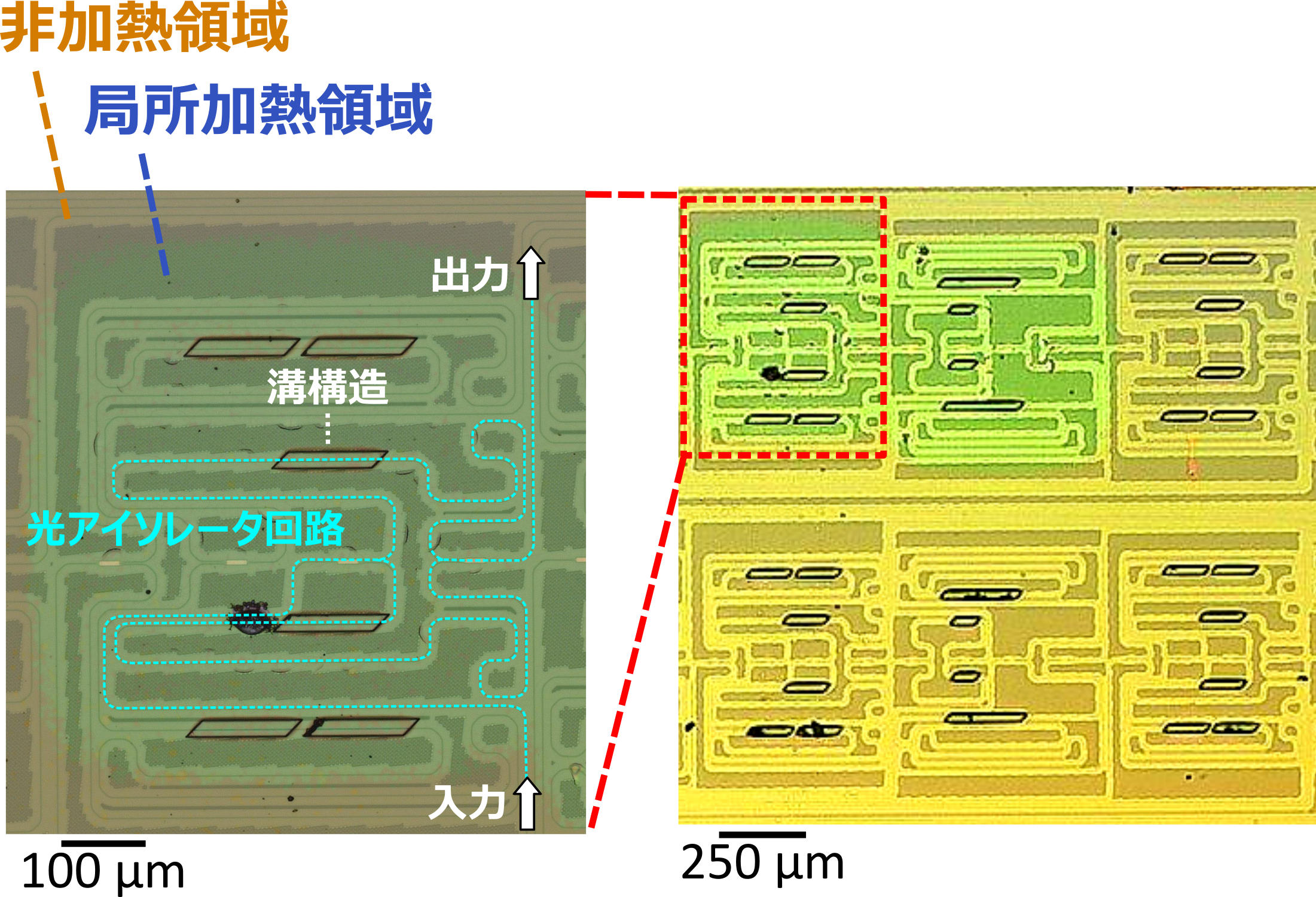
レーザーアニールを用いてシリコン光回路上に集積作製した、光アイソレータの顕微鏡画像
<関連情報>
- https://www.kyocera.co.jp/newsroom/news/2026/003040.html
- https://ieeexplore.ieee.org/document/11675811
シリコン導波路上にレーザー焼鈍した鉄ガーネットを用いたモノリシック磁気光学マッハツェンダーアイソレーター Monolithic Magneto-Optical Mach-Zehnder Isolator Using Laser-Annealed Iron Garnet on a Silicon Waveguide
Tomoya Sugita; Reona Motoji; Yuki Yoshihara; Dan Maeda; Hiroki Yamamoto; Hibiki Miyashita;Kazushi Ishiyama:Taichi Goto
IEEE Access Published:02 September 2026
DOI:https://doi.org/10.1109/ACCESS.2026.3729586
Abstract
Stable silicon photonic circuits require monolithically integrated optical isolators based on magneto-optical garnet. However, crystallizing the garnet by conventional furnace annealing exposes the entire chip to high temperature and degrades the silicon waveguides and the metal electrodes. Here we avoid this degradation by using local laser annealing in vacuum to crystallize cerium-substituted yttrium iron garnet (Ce:YIG), deposited by ion beam sputtering without a seed layer, directly within a silicon-based Mach-Zehnder interferometer. A laser beam at a wavelength of 915 nm locally crystallized the garnet in a 700 μm square region. The device achieves an isolation ratio of 13.6 dB at a wavelength of 1540 nm, corresponding to a Faraday rotation of 0.092°/μm, with an insertion loss of 20.4 dB and a propagation loss of 9.5 dB. Transmission electron microscopy reveals the crystallized Ce:YIG and a ~10 nm boundary region at the interface with the Si waveguide. These results demonstrate that magneto-optical thin films requiring high-temperature processing can be crystallized locally within a silicon photonic circuit by a high-throughput technique compatible with mass production.

