
2006-08-05 マサチューセッツ工科大学(MIT)
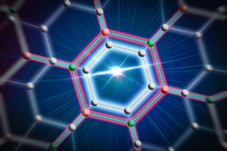
The new technique allows researchers to generate an ultrathin superconducting material (represented by pink and green spheres) underneath another anatomically thin material — carbon-based graphene (grey). Credits: Image: Jose-Luis Olivares, MIT
<関連情報>
- https://news.mit.edu/2026/researchers-make-air-stable-ultrathin-superconductors-more-scalable-quantum-devices-0805
- https://www.nature.com/articles/s41586-026-10865-1
- https://www.nature.com/articles/s41586-025-09510-0
量子回路用空気安定型2次元超伝導体のカプセル化エピタキシャル成長 Encapsulation epitaxy of air-stable 2D superconductors for quantum circuits
Xudong Zheng,Sameia Zaman,Kenan Zhang,Connor A. Occhialini,Haowei Xu,Zhien Wang,Xinyan Li,Fangyuan Liu,Luiz Gustavo Pimenta Martins,Sejoon Lim,Tianyi Zhang,Tilo H. Yang,Jiangtao Wang,Yunyue Zhu,Zachariah Hennighausen,Sein Park,Steven Vitale,Kevin Tibbetts,Stephen Margiotta,Phillip Kim,Cong Su,Yimo Han,Ju Li,Riccardo Comin,… Jing Kong
Nature Published:05 August 2026
DOI:https://doi.org/10.1038/s41586-026-10865-1
Abstract
Two-dimensional (2D) superconductors are emerging platforms supporting both strongly correlated physics and quantum information science1,2. Their reduced dimensionality, atomically flat interfaces and high crystallinity are particularly attractive for realizing compact lumped-element devices in superconducting circuits3,4,5. However, large-scale synthesis of monolayer 2D superconductors remains challenging as they are easily oxidized in air6. Here we report an ‘encapsulation epitaxy’ mechanism that enables the growth of large-area (more than 1 inch), air-stable, monolayer niobium diselenide (NbSe2) films (1L-NbSe2) and explore their potential for superconducting quantum circuits. This work represents a distinct growth phenomenon in which a 2D encapsulation layer, such as graphene or hexagonal boron nitride, pre-deposited on a 3D substrate (for example, SiO2 or Si3N4) simultaneously serves as a template for the epitaxial growth of 1L-NbSe2 underneath it at the encapsulation–substrate interface and as a protective capping layer against ambient degradation. The as-grown 1L-graphene/NbSe2 heterostructures exhibit robust superconductivity (superconducting transition temperature Tc ≈ 1 K) and enhanced charge density waves (CDWs; CDW transition temperature TCDW ≈ 177 K). We further demonstrate the integration of 1L-NbSe2 into superconducting circuits by developing oxidation-free transfer and superconducting edge-contact techniques. The 1L-NbSe2 in these circuits feature a measured kinetic inductance LK ≈ 0.7 nH □−1, making it suitable for quantum circuits requiring elements with high kinetic inductance. This encapsulation-epitaxy methodology enables the production of air-stable 2D superconductors and van der Waals heterostructures, holding promise for wafer-scale, monolithic fabrication of superconducting quantum circuitry.
静電反発に基づくファンデルワールス物質の転送 Electrostatic-repulsion-based transfer of van der Waals materials
Xudong Zheng,Jiangtao Wang,Jianfeng Jiang,Tianyi Zhang,Jiadi Zhu,Tong Dang,Peng Wu,Ang-Yu Lu,Ding-Rui Chen,Tilo H. Yang,Xinyuan Zhang,Kenan Zhang,Kyung Yeol Ma,Zhien Wang,Aijia Yao,Haomin Liu,Yi Wan,Ya-Ping Hsieh,Vladimir Bulović,Tomás Palacios & Jing Kong
Nature Published:24 September 2025
DOI:https://doi.org/10.1038/s41586-025-09510-0
Abstract
Van der Waals (vdW) materials offer unique opportunities for 3D integration1,2 of planar circuits towards higher-density transistors and energy-efficient computation3,4,5,6,7. Owing to the high thermal budget and special substrate requirement for the synthesis of high-quality vdW materials8,9,10, an advanced transfer technique is required that can simultaneously meet a broad range of industrial requirements, including high intactness, cleanliness and speed, large scale, low cost and versatility. However, previous efforts based on either etching or etching-free mechanisms typically only improve one or two of the aforementioned aspects11,12,13 and a comprehensive and systematic solution remains lacking. Here we demonstrate an electrostatic-repulsion-enabled advanced transfer technique that is etching free, high yield, fast, wafer scale, low cost and widely applicable, using ammonia solution compatible with the complementary metal–oxide–semiconductor (CMOS) industry. The high material intactness and interface cleanliness enable superior device performances in 2D field-effect transistors with 100% yield, near-zero hysteresis (7 mV) and near-ideal subthreshold swing (65.9 mV dec−1). The combination with bismuth contact further enables an ultrahigh on-current of 1.3 mA μm−1 under 1 V bias. This advanced transfer approach offers a facile and manufacturing-viable solution for vdW-materials-based electronics, paving the way for advanced 3D integration in the future.
