
2024-07-25 ペンシルベニア州立大学(PennState)
")
New work led by researchers at Penn State may provide new concepts to construct interconnects — quantum information highways — in quantum computers Credit: vchal/Getty Images. All Rights Reserved.
キンク状態とは、半導体材料の端に沿って形成される特定の電気伝導経路のことです。この現象は、特定の材料配置や電場によって引き起こされ、通常の伝導経路とは異なる電子の動きを特徴とします。
◆具体的には、キンク状態は量子バレー・ホール効果によって引き起こされます。この効果では、電子が異なる「バレー」状態に分かれ、これらの状態にある電子が異なる方向に移動します。キンク状態では、電子が互いに衝突せずに同じ経路を共有することが可能です。この特性により、電子の逆散乱が防がれ、効率的な電子伝導が実現されます。
◆ペンシルベニア州立大学の研究では、このキンク状態を制御するためのスイッチを開発し、量子情報を伝送する新しい方法を提案しています。この技術は、量子デバイスや量子コンピュータの開発において重要な進展となる可能性があります。
<関連情報>
- https://www.psu.edu/news/research/story/kink-state-control-may-provide-pathway-quantum-electronics/
- https://www.science.org/doi/10.1126/science.adj3742
- https://www.nature.com/articles/nnano.2016.158
量子化抵抗とトポロジカルスイッチを持つ高温量子バレーホール効果 High-temperature quantum valley Hall effect with quantized resistance and a topological switch
Ke Huang, Hailong Fu, Kenji Watanabe, Takashi Taniguchi, and Jun Zhu
Science Published:18 Jul 2024
DOI:https://doi.org/10.1126/science.adj3742
Abstract
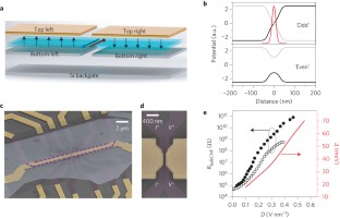
Edge states of a topological insulator can be used to explore fundamental science emerging at the interface of low dimensionality and topology. Achieving a robust conductance quantization, however, has proven challenging for helical edge states. Here we show wide resistance plateaus in kink states – a manifestation of the quantum valley Hall effect in Bernal bilayer graphene – quantized to the predicted value at zero magnetic field. The plateau resistance has a very weak temperature dependence up to 50 Kelvin and is flat within a dc bias window of tens of mV. We demonstrate the electrical operation of a topology-controlled switch with an on/off ratio of 200. These results demonstrate the robustness and tunability of the kink states and its promise in constructing electron quantum optics devices.
二層グラフェンにおけるゲート制御トポロジカル伝導チャネル Gate-controlled topological conducting channels in bilayer graphene
Jing Li,Ke Wang,Kenton J. McFaul,Zachary Zern,Yafei Ren,Kenji Watanabe,Takashi Taniguchi,Zhenhua Qiao & Jun Zhu
Nature Nanotechnology Published:29 August 2016
DOI:https://doi.org/10.1038/nnano.2016.158
Abstract
The existence of inequivalent valleys K and K′ in the momentum space of 2D hexagonal lattices provides a new electronic degree of freedom, the manipulation of which can potentially lead to new types of electronics, analogous to the role played by electron spin1,2,3. In materials with broken inversion symmetry, such as an electrically gated bilayer graphene (BLG)4,5, the momentum-space Berry curvature Ω carries opposite sign in the K and K′ valleys. A sign reversal of Ω along an internal boundary of the sheet gives rise to counterpropagating 1D conducting modes encoded with opposite-valley indices. These metallic states are topologically protected against backscattering in the absence of valley-mixing scattering, and thus can carry current ballistically1,6,7,8,9,10,11. In BLG, the reversal of Ω can occur at the domain wall of AB- and BA-stacked domains12,13,14, or at the line junction of two oppositely gated regions6. The latter approach can provide a scalable platform to implement valleytronic operations, such as valves and waveguides9,15, but it is technically challenging to realize. Here, we fabricate a dual-split-gate structure in BLG and present evidence of the predicted metallic states in electrical transport. The metallic states possess a mean free path (MFP) of up to a few hundred nanometres in the absence of a magnetic field. The application of a perpendicular magnetic field suppresses the backscattering significantly and enables a junction 400 nm in length to exhibit conductance close to the ballistic limit of 4e2/h at 8 T. Our experiment paves the way to the realization of gate-controlled ballistic valley transport and the development of valleytronic applications in atomically thin materials.

")
