2023-12-06 デンマーク工科大学(DTU)
◆シリコン構造の半分をスプリングで浮かせ、選択的なガラスエッチングにより生成された共振器は、史上最小のサイズで光を長時間保存し、光学チップに組み込むことが可能です。これはトップダウンとボトムアップのアプローチを融合し、ナノテクノロジーの可能性を拓く先駆的な一歩です。
<関連情報>
- https://www.dtu.dk/english/news/all-news/bowtie-resonators-that-build-themselves-bridge-the-gap-between-nanoscopic-and-macroscopic
- https://www.nature.com/articles/s41586-023-06736-8
原子スケールの閉じ込めを持つ自己組織化フォトニック共振器 Self-assembled photonic cavities with atomic-scale confinement
Ali Nawaz Babar,Thor August Schimmell Weis,Konstantinos Tsoukalas,Shima Kadkhodazadeh,Guillermo Arregui,Babak Vosoughi Lahijani & Søren Stobbe
Nature Published:06 December 2023
DOI:https://doi.org/10.1038/s41586-023-06736-8

Abstract
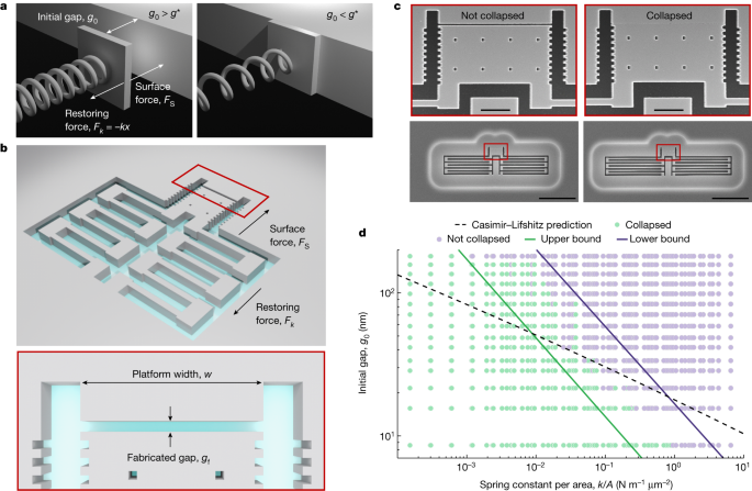
Despite tremendous progress in research on self-assembled nanotechnological building blocks, such as macromolecules1, nanowires2 and two-dimensional materials3, synthetic self-assembly methods that bridge the nanoscopic to macroscopic dimensions remain unscalable and inferior to biological self-assembly. By contrast, planar semiconductor technology has had an immense technological impact, owing to its inherent scalability, yet it seems unable to reach the atomic dimensions enabled by self-assembly. Here, we use surface forces, including Casimir–van der Waals interactions4, to deterministically self-assemble and self-align suspended silicon nanostructures with void features well below the length scales possible with conventional lithography and etching5, despite using only conventional lithography and etching. The method is remarkably robust and the threshold for self-assembly depends monotonically on all the governing parameters across thousands of measured devices. We illustrate the potential of these concepts by fabricating nanostructures that are impossible to make with any other known method: waveguide-coupled high-Q silicon photonic cavities6,7 that confine telecom photons to 2 nm air gaps with an aspect ratio of 100, corresponding to mode volumes more than 100 times below the diffraction limit. Scanning transmission electron microscopy measurements confirm the ability to build devices with sub-nanometre dimensions. Our work constitutes the first steps towards a new generation of fabrication technology that combines the atomic dimensions enabled by self-assembly with the scalability of planar semiconductors.


