次世代エレクトロニクスに期待される立方晶ヒ化ホウ素の高キャリア移動度 High Carrier Mobility in Cubic Boron Arsenide Offers Promise for Next-Gen Electronics
2022-07-21 ヒューストン大学(UH)

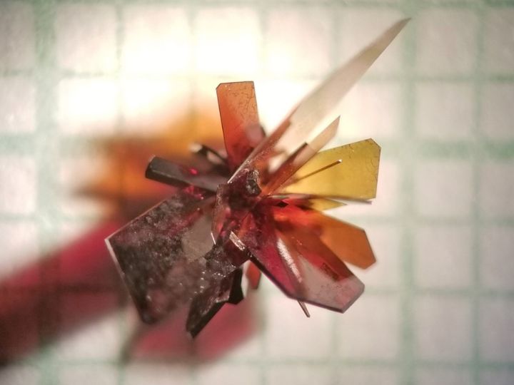
Boron Arsenide Single Crystals
この結晶は、電子と正孔の移動度が同時に高くなることが以前から予想されていましたが、『Science』誌に掲載された2本の論文のうちの1本は、室温での高いキャリア移動度を実験的に検証し、商用アプリケーションへの応用の可能性を広げたことを示しています。
『Science』誌に掲載された付随論文では、過渡反射顕微鏡を使って結晶を測定し、高い移動度を実証し、より高エネルギーのレーザービームを使用した場合には、以前の予測を上回る場合もあったことが述べられています。
<関連情報>
- https://uh.edu/news-events/stories/2022-news-articles/july-2022/07212022-semiconductor-materials.php
- https://www.science.org/doi/10.1126/science.abn4290
- https://www.science.org/doi/10.1126/science.abn4727
立方晶ヒ化ホウ素における高い両極性移動度 High ambipolar mobility in cubic boron arsenide
Jungwoo Shin,Geethal Amila Gamage,Zhiwei Ding,Ke Chen,Fei Tian ,Xin Qian,Jiawei Zhou ,Hwijong Lee ,Jianshi Zhou,Li Shi ,Thanh Nguyen ,Fei Han,Mingda Li,David Broido ,Aaron Schmidt,Zhifeng Ren,Gang Chen
Science Published:21 Jul 2022
DOI:DOI: 10.1126/science.abn4290
Swift carriers
Boron arsenide is a semiconductor with several interesting properties, including a high thermal conductivity. Theoretical calculations also suggest that it has high ambipolar mobility, a measure of the mobility of electrons and holes. Yue et al. and Shin et al. used different types of measurements to observe a high ambipolar mobility in very pure cubic boron arsenide. Shin et al. were able to simultaneously measure the high thermal and electrical transport properties in the same place in their samples. Yue et al. found even higher ambipolar mobility than the theoretical estimates at a few locations. Boron arsenide’s combination of transport properties could make it an attractive semiconductor for various applications. —BG
Abstract
Semiconductors with high thermal conductivity and electron-hole mobility are of great importance for electronic and photonic devices as well as for fundamental studies. Among the ultrahigh–thermal conductivity materials, cubic boron arsenide (c-BAs) is predicted to exhibit simultaneously high electron and hole mobilities of >1000 centimeters squared per volt per second. Using the optical transient grating technique, we experimentally measured thermal conductivity of 1200 watts per meter per kelvin and ambipolar mobility of 1600 centimeters squared per volt per second at the same locations on c-BAs samples at room temperature despite spatial variations. Ab initio calculations show that lowering ionized and neutral impurity concentrations is key to achieving high mobility and high thermal conductivity, respectively. The high ambipolar mobilities combined with the ultrahigh thermal conductivity make c-BAs a promising candidate for next-generation electronics.
過渡反射率顕微鏡による立方晶ヒ化ホウ素の高い両極移動度の解明 High ambipolar mobility in cubic boron arsenide revealed by transient reflectivity microscopy
Shuai Yue,Fei Tian,Xinyu Sui,Mohammadjavad Mohebinia,Xianxin Wu,Tian Tong,Zhiming Wang,Bo Wu ,Qing Zhang ,Zhifeng Ren,Jiming Bao,Xinfeng Liu
Science Published:21 Jul 2022
DOI: 10.1126/science.abn4727
Swift carriers
Boron arsenide is a semiconductor with several interesting properties, including a high thermal conductivity. Theoretical calculations also suggest that it has high ambipolar mobility, a measure of the mobility of electrons and holes. Yue et al. and Shin et al. used different types of measurements to observe a high ambipolar mobility in very pure cubic boron arsenide. Shin et al. were able to simultaneously measure the high thermal and electrical transport properties in the same place in their samples. Yue et al. found even higher ambipolar mobility than the theoretical estimates at a few locations. Boron arsenide’s combination of transport properties could make it an attractive semiconductor for various applications. —BG
Abstract
Semiconducting cubic boron arsenide (c-BAs) has been predicted to have carrier mobility of 1400 square centimeters per volt-second for electrons and 2100 square centimeters per volt-second for holes at room temperature. Using pump-probe transient reflectivity microscopy, we monitored the diffusion of photoexcited carriers in single-crystal c-BAs to obtain their mobility. With near-bandgap 600-nanometer pump pulses, we found a high ambipolar mobility of 1550 ± 120 square centimeters per volt-second, in good agreement with theoretical prediction. Additional experiments with 400-nanometer pumps on the same spot revealed a mobility of >3000 square centimeters per volt-second, which we attribute to hot electrons. The observation of high carrier mobility, in conjunction with high thermal conductivity, enables an enormous number of device applications for c-BAs in high-performance electronics and optoelectronics.


