2026-04-08 アメリカ合衆国・カリフォルニア大学サンディエゴ校(UCSD)

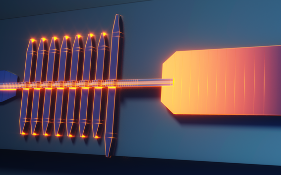
A chip designed to convert high voltages into lower levels in electronics — a process known as DC-DC step-down conversion — more efficiently using a piezoelectric resonator. Photos by David Baillot/UC San Diego Jacobs School of Engineering
<関連情報>
- https://today.ucsd.edu/story/new-chip-design-could-boost-efficiency-of-power-management-in-data-centers
- https://www.nature.com/articles/s41467-026-70494-0
ハイブリッド圧電共振器ベースのDC-DCコンバータ A hybrid piezoelectric resonator-based DC-DC converter
Jae-Young Ko,Wen-Chin B. Liu & Patrick P. Mercier
Nature Communications Published:17 March 2026
DOI:https://doi.org/10.1038/s41467-026-70494-0
Abstract
Piezoelectric resonators are becoming attractive alternatives to conventional magnetics in DC-DC converters due to their favorable scaling and manufacturing properties. However, the efficiency and current handling capabilities of baseline piezoelectric resonator-based DC-DC converters degrade at higher voltage conversion ratios due to charge utilization limitations imposed by topological operation. Here we present an Always-Multi-Path Embedded Flying Capacitor Piezoelectric Resonator-based DC-DC converter that uses flying capacitors to add both hybrid multi-path output power delivery features and to reduce the internal charge redistribution losses within the piezoelectric resonator. Specifically, the proposed integrated circuit modifies the optimal voltage conversion of the piezo network from 2:1 to 3:1 while adding a switched-capacitor output network that enables multi-path operation at all times, resulting in a net optimal voltage conversion ratio of 9:1 for the converter, with 4x improved output current. Fabricated in a 180 nm high-voltage CMOS process, the developed chip achieves a peak efficiency of 96.2% at a 48-to-4.8 V conversion ratio.