203-11-09 NASA

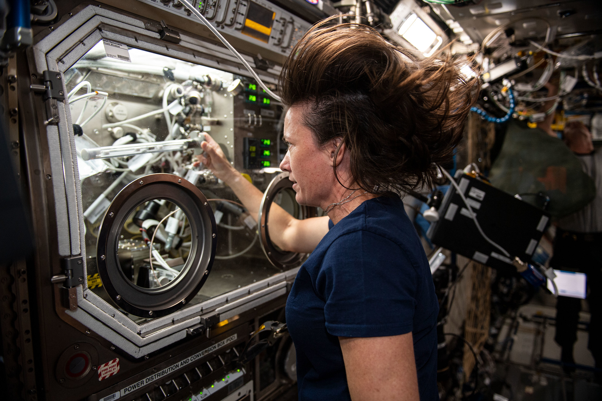
NASA astronaut and Expedition 65 Flight Engineer Megan McArthur works in the Microgravity Science Glovebox swapping samples for an experiment called Solidification Using a Baffle in Sealed Ampoules, or SUBSA. The physics investigation explores experimental methods of crystallizing melts in microgravity and is expected to result in reduced fluid motion in the melt, leading to better distribution of subcomponents and the potential for improved technology used in producing semiconductor crystals. NASA
◆さらに、地球周回軌道(LEO)での製造は実用的な利点があり、NASAのInSPAの目標達成につながると主張されている。これには、米国の技術リーダーシップ強化や国家安全保障の向上、高品質の雇用創出、人類への利益提供、そしてLEOでの強固な経済の発展が含まれる。
<関連情報>
- https://www.nasa.gov/general/the-benefits-of-semiconductor-manufacturing-in-low-earth-orbit-leo-for-terrestrial-use/
- https://osf.io/d6ar4/
地球低軌道での地上用半導体製造 Semiconductor Manufacturing in Low-Earth Orbit for Terrestrial Use
Jessica Frick,Erik Kulu,Gary Rodrigue,Curtis Hill,Debbie Senesky
OSF Preprints
Abstract
In-space manufacturing offers technological innovation, advancements, and discoveries unbound by Earth’s gravitational forces. To harness the full potential of manufacturing in low-Earth orbit (LEO), industry leaders gathered at Stanford University in March 2023 at the inaugural Semiconductor Manufacturing in the Space Domain Workshop to discuss the past, present, and future of the field. This workshop brought together a community of experts to explore the rich history of semiconductor and in-space manufacturing. These experts and their foundational research and collaboration are the driving force behind this paper. The workshop’s priority was to identify the 2030 goals that must be reached to make in-space semiconductor production a reality by 2050. The consensus was that the field needs to take the remaining years to de- risk investment from semiconductor corporations and private investors. To do that, the community needs to obtain more iterative data on promising semiconductor R&D in LEO. This would include the whole range of experiments in the semiconductor production phases such as crystal growth, wafer processing, epitaxial growth, circuit patterning, etc. Beyond synthesizing the takeaways from the workshop, the report describes the current state of semiconductor manufacturing in space and carves out a path for the future. Over the past three decades, the deteriorating discovery and growth of crystalline materials (DGCM) capacity in the United States has significantly stalled the domestic semiconductor industry. This report intends to regain U.S. attention to space-based semiconductor manufacturing and bring the field back from hibernation. The Vision for 2050 and Call to Action sections, informed by both industry and history experts, propose actionable solutions that can awaken the semiconductor industry from nearly 25 years of inactivity in space. The benefits of semiconductor manufacturing in LEO are clear. Earth’s gravitational forces pose substantial barriers to quick, high-yield semiconductor production. Beyond the scientific benefits of microgravity, there are substantial practical benefits to incorporating LEO-based manufacturing into the supply chain. Transitioning this industry into space is the only path forward if the United States is to keep pace with the technological arms race unfolding across the globe. This report identifies opportunities to strengthen U.S. leadership in the LEO-based semiconductor manufacturing field. The industry urgently needs a roadmap for both immediate and long-term funding strategies that can support various components. Long- term government investments can help de-risk additional private investments, and funding student fellowship programs will drive workforce development. Beyond a need for funding, the industry needs a designated collaborative community ecosystem. This field is currently situated alongside several related fields, and gaining traction in established fields is certainly necessary. However, there is a clear need for a designated “home” and community that can draw on knowledge from academia, the space sector, and the semiconductor industry. A push towards this collaborative environment will only benefit the industry at large and give the United States a competitive edge in this growing field. This paper will explain the scientific basis for this industry in the proceeding sections. Discussions of the past and present of semiconductor manufacturing in LEO will provide the necessary context for the various author recommendations to develop the industry.


