光あれ (Let there be (controlled) light)")
2023-02-23 ドイツ連邦共和国・ヘルマン・フォン・ヘルムホルツ協会(HGF)
・ ヘルツホルムセンター・ドレスデン・ロッセンドルフ研究所(HZDR)、ドレスデン工科大学(TU Dresden)お
よびライプニッツ結晶成長研究所(IKZ)が、シリコンウェハーの任意の場所にシングルフォトンエミッターをモノリシックに集積するナノファブリケーション技術を開発。
・ 様々な光コンポーネントを搭載した光集積回路(PICs)の単一チップ上での光の生成、送信、処理や検出機能は、量子コンピューティングのような次世代技術で重要な役割を担う。
・ 量子ビット(光量子状態)を効果的に制御できる PICs は、データベース検索、AI システムやシミュレーションのような新しいアプローチでのコンピューティングの革新が期待される、量子コンピューターに不可欠なもの。
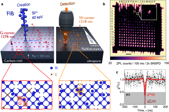
・ 液体金属合金のイオン源による集束イオンビーム(FIB)を使用した製造方法で、シリコンウェハー上の任意の場所にフォトンエミッターを配置し、高収率と高スペクトル品質を達成。また、CMOS 技術に適応するスケーラブルなブロードビーム注入も実証した。
・ 冷却と加熱の複数回のサイクルによる材料試験後も光特性の維持を確認。今後の大量生産に向けた要件となり、産業スケールのフォトニック量子プロセッサ製造の可能性を拓く。同シングルフォトンエミッターは、ファウンドリでの製造や既存の通信インフラへの導入が技術的に可能。
URL: https://www.hzdr.de/db/Cms?pNid=99&pOid=68184
<NEDO海外技術情報より>
関連情報
Nature Communications 掲載論文(フルテキスト)
Wafer-scale nanofabrication of telecom single-photon emitters in silicon
URL: https://www.nature.com/articles/s41467-022-35051-5
Abstract
A highly promising route to scale millions of qubits is to use quantum photonic integrated circuits (PICs), where deterministic photon sources, reconfigurable optical elements, and single-photon detectors are monolithically integrated on the same silicon chip. The isolation of single-photon emitters, such as the G centers and W centers, in the optical telecommunication O-band, has recently been realized in silicon. In all previous cases, however, single-photon emitters were created uncontrollably in random locations, preventing their scalability. Here, we report the controllable fabrication of single G and W centers in silicon wafers using focused ion beams (FIB) with high probability. We also implement a scalable, broad-beam implantation protocol compatible with the complementary-metal-oxide-semiconductor (CMOS) technology to fabricate single telecom emitters at desired positions on the nanoscale. Our findings unlock a clear and easily exploitable pathway for industrial-scale photonic quantum processors with technology nodes below 100 nm.
除菌の有効性を確認~新たなUV活用ソリューションの開発に向け、今治市公会堂で実証実験を実施、座席表面の除菌効果を確認~")
")