2025-03-21 コロンビア大学
<関連情報>
- https://www.engineering.columbia.edu/about/news/new-study-showcases-3d-photonics-record-performance-ai
- https://www.nature.com/articles/s41566-025-01633-0
超低エネルギー、高帯域幅のチップ間データリンクのための3次元フォトニック集積化 Three-dimensional photonic integration for ultra-low-energy, high-bandwidth interchip data links
Stuart Daudlin,Anthony Rizzo,Sunwoo Lee,Devesh Khilwani,Christine Ou,Songli Wang,Asher Novick,Vignesh Gopal,Michael Cullen,Robert Parsons,Kaylx Jang,Alyosha Molnar & Keren Bergman
Nature Photonics Published:21 March 2025
DOI:https://doi.org/10.1038/s41566-025-01633-0

Abstract
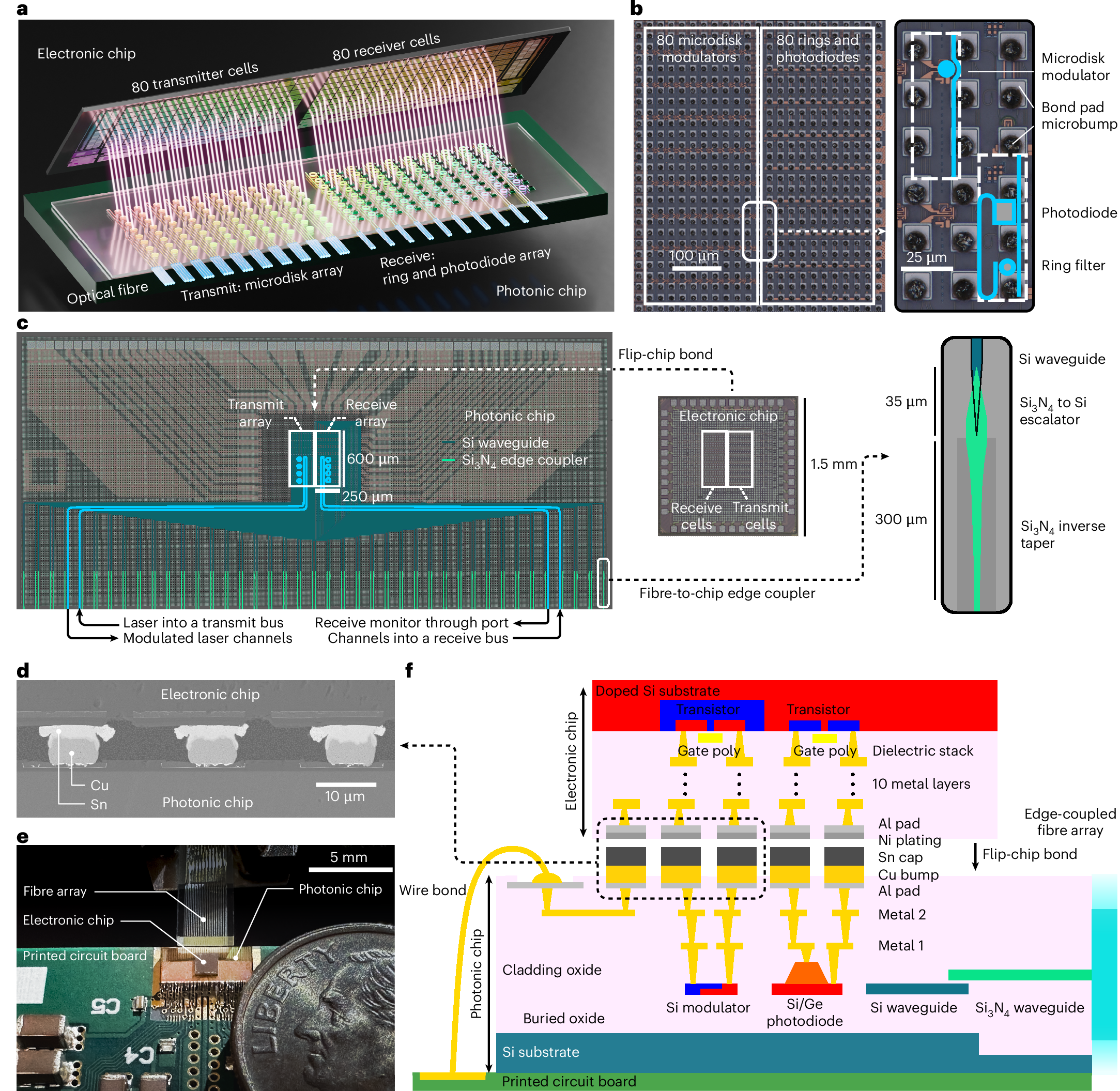
Artificial intelligence (AI) hardware is positioned to unlock revolutionary computational abilities by leveraging vast distributed networks of advanced semiconductor chips. However, a barrier for AI scaling is the disproportionately high energy and chip area required to transmit data between the chips. Here we present a solution to this long-standing overhead through dense three-dimensional (3D) integration of photonics and electronics. With 80 photonic transmitters and receivers occupying a combined chip footprint of only 0.3 mm2, our platform achieves an order-of-magnitude-greater number of 3D-integrated channels than prior demonstrations. This enables both high-bandwidth (800 Gb s−1) and highly efficient, dense (5.3 Tb s−1 mm−2) 3D channels. The transceiver energy efficiency is showcased by a state-of-the-art 50 fJ and 70 fJ per communicated bit from the transmitter and receiver front ends, respectively, operating at 10 Gb s−1per channel. Furthermore, the design is compatible with commercial complementary metal–oxide–semiconductor foundries fabrication on 300-mm-sized wafers, providing a route to mass production. Such ultra-energy-efficient, high-bandwidth data communication links promise to eliminate the bandwidth bottleneck between spatially distinct compute nodes and support the scaling of future AI computing hardware.


