2024-11-04 マサチューセッツ工科大学(MIT)
<関連情報>
- https://news.mit.edu/2024/nanoscale-transistors-could-enable-more-efficient-electronics-1104
- https://www.nature.com/articles/s41928-024-01279-w
極端な量子閉じ込めを持つ、スケールアップした垂直ナノワイヤーヘテロ接合トンネル・トランジスタ Scaled vertical-nanowire heterojunction tunnelling transistors with extreme quantum confinement
Yanjie Shao,Marco Pala,Hao Tang,Baoming Wang,Ju Li,David Esseni & Jesús A. del Alamo
Nature Electronics Published:04 November 2024
DOI:https://doi.org/10.1038/s41928-024-01279-w

Abstract
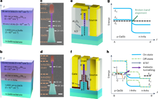
The development of data-centric computing requires new energy-efficient electronics that can overcome the fundamental limitations of conventional silicon transistors. A range of novel transistor concepts have been explored, but an approach that can simultaneously offer high drive current and steep slope switching while delivering the necessary scaling in footprint is still lacking. Here, we report scaled vertical-nanowire heterojunction tunnelling transistors that are based on the broken-band GaSb/InAs system. The devices offer a drive current of 300 µA µm−1 and a sub-60 mV dec−1 switching slope at an operating voltage of 0.3 V. The approach relies on extreme quantum confinement at the tunnelling junction and is based on an interface-pinned energy band alignment at the tunnelling heterojunction under strong quantization.


