2024-09-24 オークリッジ国立研究所(ORNL)

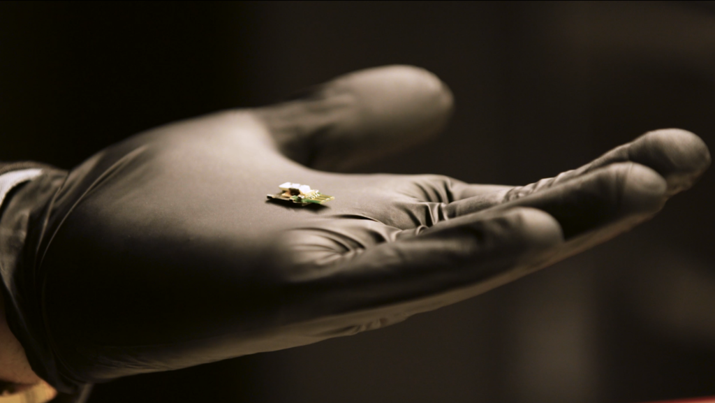
A heater platform was designed to deliver atomized material to a sample, converting a scanning transmission electron microscope into a synthescope. Credit: Ondrej Dyck/ORNL, U.S. Dept. of Energy.
<関連情報>
- https://www.ornl.gov/news/writing-atoms-could-transform-materials-fabrication-quantum-devices
- https://onlinelibrary.wiley.com/doi/10.1002/adma.202302906
ツイスト二層グラフェンにおける原子パターンのトップダウン作製 Top-Down Fabrication of Atomic Patterns in Twisted Bilayer Graphene
Ondrej Dyck, Sinchul Yeom, Andrew R. Lupini, Jacob L. Swett, Dale Hensley, Mina Yoon, Stephen Jesse
Advanced Materials Published: 13 June 2023
DOI:https://doi.org/10.1002/adma.202302906
Abstract
Atomic-scale engineering typically involves bottom-up approaches, leveraging parameters such as temperature, partial pressures, and chemical affinity to promote spontaneous arrangement of atoms. These parameters are applied globally, resulting in atomic-scale features scattered probabilistically throughout the material. In a top-down approach, different regions of the material are exposed to different parameters, resulting in structural changes varying on the scale of the resolution. In this work, the application of global and local parameters is combined in an aberration-corrected scanning transmission electron microscope (STEM) to demonstrate atomic-scale precision patterning of atoms in twisted bilayer graphene. The focused electron beam is used to define attachment points for foreign atoms through the controlled ejection of carbon atoms from the graphene lattice. The sample environment is staged with nearby source materials such that the sample temperature can induce migration of the source atoms across the sample surface. Under these conditions, the electron-beam (top-down) enables carbon atoms in the graphene to be replaced spontaneously by diffusing adatoms (bottom-up). Using image-based feedback control, arbitrary patterns of atoms and atom clusters are attached to the twisted bilayer graphene with limited human interaction. The role of substrate temperature on adatom and vacancy diffusion is explored by first-principles simulations.
原子ごとの直接書き込み Atom-by-Atom Direct Writing
Ondrej DyckAndrew R. Lupini and Stephen Jesse
Nano Letters Published: March 6, 2023
DOI:https://doi.org/10.1021/acs.nanolett.3c00114
Abstract

Direct-write processes enable the alteration or deposition of materials in a continuous, directable, sequential fashion. In this work, we demonstrate an electron beam direct-write process in an aberration-corrected scanning transmission electron microscope. This process has several fundamental differences from conventional electron-beam-induced deposition techniques, where the electron beam dissociates precursor gases into chemically reactive products that bond to a substrate. Here, we use elemental tin (Sn) as a precursor and employ a different mechanism to facilitate deposition. The atomic-sized electron beam is used to generate chemically reactive point defects at desired locations in a graphene substrate. Temperature control of the sample is used to enable the precursor atoms to migrate across the surface and bond to the defect sites, thereby enabling atom-by-atom direct writing.


