2024-01-10 ペンシルベニア州立大学(PennState)
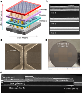
◆研究では、2D材料で作られたトランジスタを含む3D統合が可能であり、これにより計算能力向上だけでなく、異なる層で多様な機能を実現できると報告されています。この手法はエネルギー効率も向上させ、将来の電子デバイスの進化に寄与する可能性があります。
<関連情報>
- https://www.psu.edu/news/materials-research-institute/story/integrating-dimensions-get-more-out-moores-law-and-advance/
- https://www.nature.com/articles/s41586-023-06860-5
2次元電界効果トランジスタの3次元集積化 Three-dimensional integration of two-dimensional field-effect transistors
Darsith Jayachandran,Rahul Pendurthi,Muhtasim Ul Karim Sadaf,Najam U Sakib,Andrew Pannone,Chen Chen,Ying Han,Nicholas Trainor,Shalini Kumari,Thomas V. Mc Knight,Joan M. Redwing,Yang Yang & Saptarshi Das
Nature Published:10 January 2024
DOI:https://doi.org/10.1038/s41586-023-06860-5

Abstract
In the field of semiconductors, three-dimensional (3D) integration not only enables packaging of more devices per unit area, referred to as ‘More Moore’1 but also introduces multifunctionalities for ‘More than Moore’2 technologies. Although silicon-based 3D integrated circuits are commercially available3,4,5, there is limited effort on 3D integration of emerging nanomaterials6,7 such as two-dimensional (2D) materials despite their unique functionalities7,8,9,10. Here we demonstrate (1) wafer-scale and monolithic two-tier 3D integration based on MoS2 with more than 10,000 field-effect transistors (FETs) in each tier; (2) three-tier 3D integration based on both MoS2 and WSe2 with about 500 FETs in each tier; and (3) two-tier 3D integration based on 200 scaled MoS2 FETs (channel length, LCH = 45 nm) in each tier. We also realize a 3D circuit and demonstrate multifunctional capabilities, including sensing and storage. We believe that our demonstrations will serve as the foundation for more sophisticated, highly dense and functionally divergent integrated circuits with a larger number of tiers integrated monolithically in the third dimension.


