2025-09-24 北京大学(PKU)

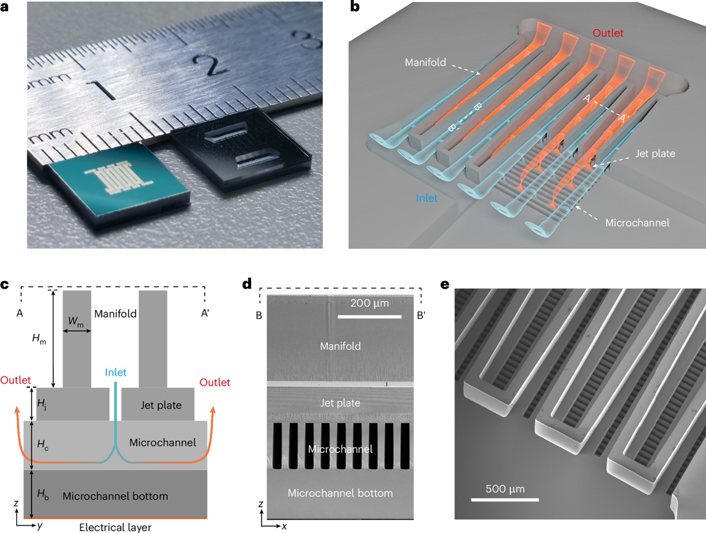
Figure 1. Jet-enhanced manifold microchannels for embedded chip cooling.
<関連情報>
- https://newsen.pku.edu.cn/news_events/news/research/15238.html
- https://www.nature.com/articles/s41928-025-01449-4
最大熱流束3,000 W cm −2までの電子機器冷却用ジェット強化マニホールドマイクロチャネル Jet-enhanced manifold microchannels for cooling electronics up to a heat flux of 3,000 W cm−2
Zhihu Wu,Wei Xiao,Haiyu He,Wei Wang & Bai Song
Nature Electronics Published:09 September 2025
DOI:https://doi.org/10.1038/s41928-025-01449-4
Abstract
The miniaturization of advanced electronics can lead to high heat fluxes, which must be dissipated before they cause device degradation or failure. Embedded microfluidic cooling is of potential value in such systems, but devices are typically limited to heat fluxes below 2,000 W cm−2. Here we report a microfluidic cooling strategy that can dissipate heat fluxes up to 3,000 W cm−2 at a pumping power of only 0.9 W cm−2 using single-phase water as the coolant. Our approach is based on a three-tier structure that consists of a tapered manifold layer on the top, a microjet layer in the middle and a microchannel layer with sawtooth-shaped sidewalls at the bottom. The structures are etched directly into the backside of the silicon substrate using standard microelectromechanical system technology. Moreover, the coefficient of performance can reach 13,000 and dissipate a heat flux of 1,000 W cm−2 at a maximum chip temperature rise of 65 K.


