2025-12-02 ヒューストン大学

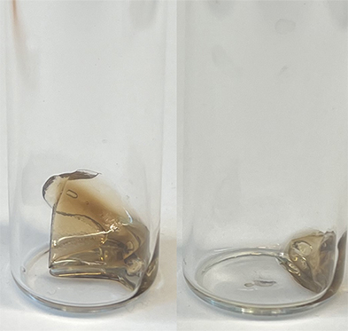
This is the two-dimensional thin film electric insulator designed in a University of Houston lab to make AI faster and reduce power consumption.
<関連情報>
- https://www.uh.edu/news-events/stories/2025/december/12022025-karim-tech-thin-film-ai-faster.php
- https://pubs.acs.org/doi/full/10.1021/acsnano.5c11582
高誘電強度、電気的および熱機械的に安定した低誘電率誘電体のための二次元共有結合有機フレームワーク膜 Two-Dimensional Covalent Organic Framework Films for High Dielectric Strength Electrically and Thermo-Mechanically Stable Low Permittivity Dielectrics
Maninderjeet Singh,Rajpiraveen Parthiban,Erin M. Schroeder,Saurabh Kumar Tiwary,Maria Camila Belduque Correa,Francisco C. Robles Hernandez,Devin L. Shaffer,and Alamgir Karim
ACS Nano Published: October 14, 2025
DOI:https://doi.org/10.1021/acsnano.5c11582
Abstract

There is an urgent need to develop advanced dielectric materials with low permittivities (κ < 1.6) to address performance-limiting challenges for conventional and artificial intelligence (AI) microprocessors with miniaturized feature sizes, namely, delay in processing speeds, electronic crosstalk, high power consumption, and charge buildup. Known low-κ materials show poor dielectric strength and thermo-mechanical properties, rendering them unsuitable for next-generation electronic devices. Here, we demonstrate that the two-dimensional (2D) covalent organic frameworks (COF) films synthesized by the liquid–liquid interfacial reaction show very low permittivities (κ ≈ 1.17 at 100 kHz), ultrahigh dielectric strengths of ≈ 3908 MV/m at room temperature (≈2100 MV/m at 300 °C), low density of ≈1.1 g/cm3, and a high Young’s modulus of ≈3.4 GPa. These properties are enabled by the highly crystalline and tightly packed nanoporous nanosheets of 2D COFs arranged in periodic structures in 2D COF films and surpass the requirements for next-generation electronic devices.


