2025-04-05 復旦大学
<関連情報>
- https://www.fudan.edu.cn/en/2025/0405/c344a144825/page.htm
- https://www.nature.com/articles/s41586-025-08759-9
二次元半導体をベースにしたRISC-V 32ビットマイクロプロセッサ A RISC-V 32-bit microprocessor based on two-dimensional semiconductors
Mingrui Ao,Xiucheng Zhou,Xinjie Kong,Saifei Gou,Sifan Chen,Xiangqi Dong,Yuxuan Zhu,Qicheng Sun,Zhejia Zhang,Jinshu Zhang,Qiran Zhang,Yan Hu,Chuming Sheng,Kaixuan Wang,Shuiyuan Wang,Jing Wan,Jun Han,Wenzhong Bao &Peng Zhou
Nature Published:02 April 2025
DOI:https://doi.org/10.1038/s41586-025-08759-9

Abstract
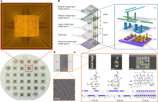
Recently the quest for post-silicon semiconductors has escalated owing to the inherent limitations of conventional bulk semiconductors, which are plagued by issues such as drain-induced barrier lowering, interfacial-scattering-induced mobility degradation and a constrained current on/off ratio determined by semiconductor bandwidth. These challenges have prompted the search for more advanced materials, with atomic-layer-thick two-dimensional (2D) semiconductors emerging as a potential solution. Following over a decade of research advances, recent developments in wafer-scale growth and device fabrication have led to breakthroughs in 2D semiconductor electronics. However, the level of integration remains constrained to a few hundred transistors. We describe a reduced instruction set computing architecture (RISC-V) microprocessor capable of executing standard 32-bit instructions on 5,900 MoS2 transistors and a complete standard cell library based on 2D semiconductor technology. The library contains 25 types of logic units. In alignment with advances in silicon integrated circuits, we also co-optimized the process flow and design of the 2D logic circuits. Our combined manufacturing and design methodology has overcome the significant challenges associated with wafer-scale integration of 2D circuits and enabled a pioneering prototype of an MoS2 microprocessor that exemplifies the potential of 2D integrated-circuit technology beyond silicon.


