
")
2024-07-05 スイス連邦工科大学ローザンヌ校(EPFL)
<関連情報>
- https://actu.epfl.ch/news/a-2d-device-for-quantum-cooling-2/
- https://www.nature.com/articles/s41565-024-01717-y
二次元ファンデルワールスヘテロ構造における電気的に調整可能な巨大ネルンスト効果 Electrically tunable giant Nernst effect in two-dimensional van der Waals heterostructures
Gabriele Pasquale,Zhe Sun,Guilherme Migliato Marega,Kenji Watanabe,Takashi Taniguchi & Andras Kis
Nature Nanotechnology Published:02 July 2024
DOI:https://doi.org/10.1038/s41565-024-01717-y
Abstract
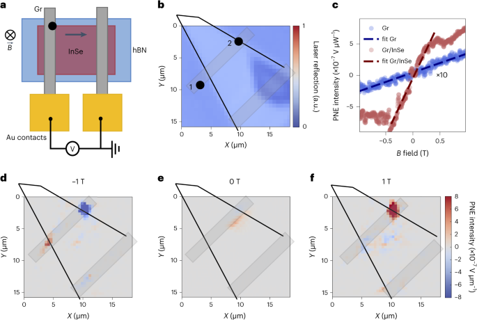
The Nernst effect, a transverse thermoelectric phenomenon, has attracted significant attention for its potential in energy conversion, thermoelectrics and spintronics. However, achieving high performance and versatility at low temperatures remains elusive. Here we demonstrate a large and electrically tunable Nernst effect by combining the electrical properties of graphene with the semiconducting characteristics of indium selenide in a field-effect geometry. Our results establish a new platform for exploring and manipulating this thermoelectric effect, showcasing the first electrical tunability with an on/off ratio of 103. Moreover, photovoltage measurements reveal a stronger photo-Nernst signal in the graphene/indium selenide heterostructure compared with individual components. Remarkably, we observe a record-high Nernst coefficient of 66.4 μV K−1 T−1 at ultralow temperatures and low magnetic fields, an important step towards applications in quantum information and low-temperature emergent phenomena.


")