2023-08-01 ミネソタ大学
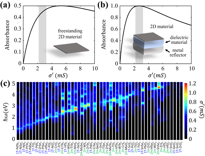
◆バンドネスティングという技術を使用し、わずか2〜3層の原子からなる材料の電気特性を操作することで「ほぼ完全な吸収体」を実現しました。この製造方法は簡単で低コストであり、他の光吸収材料と比べて拡大が容易です。研究は、「Nature Communications」誌に掲載されており、光通信などの分野で高速で効率的な光通信を可能にする可能性があります。
<関連情報>
- https://cse.umn.edu/college/news/research-brief-umn-led-team-achieves-near-perfect-light-absorption-atomic-scale
- https://www.nature.com/articles/s41467-023-39450-0
原子レベルの薄さの遷移金属ジカルコゲナイドにおいて、バンドネスティングによりほぼ完全な光吸収を達成 Achieving near-perfect light absorption in atomically thin transition metal dichalcogenides through band nesting
Seungjun Lee,Dongjea Seo,Sang Hyun Park,Nezhueytl Izquierdo,Eng Hock Lee,Rehan Younas,Guanyu Zhou,Milan Palei,Anthony J. Hoffman,Min Seok Jang,Christopher L. Hinkle,Steven J. Koester & Tony Low
Nature Communications Published:01 July 2023
DOI:https://doi.org/10.1038/s41467-023-39450-0

Abstract
Near-perfect light absorbers (NPLAs), with absorbance, A, of at least 99%, have a wide range of applications ranging from energy and sensing devices to stealth technologies and secure communications. Previous work on NPLAs has mainly relied upon plasmonic structures or patterned metasurfaces, which require complex nanolithography, limiting their practical applications, particularly for large-area platforms. Here, we use the exceptional band nesting effect in TMDs, combined with a Salisbury screen geometry, to demonstrate NPLAs using only two or three uniform atomic layers of transition metal dichalcogenides (TMDs). The key innovation in our design, verified using theoretical calculations, is to stack monolayer TMDs in such a way as to minimize their interlayer coupling, thus preserving their strong band nesting properties. We experimentally demonstrate two feasible routes to controlling the interlayer coupling: twisted TMD bi-layers and TMD/buffer layer/TMD tri-layer heterostructures. Using these approaches, we demonstrate room-temperature values of A=95% at λ=2.8 eV with theoretically predicted values as high as 99%. Moreover, the chemical variety of TMDs allows us to design NPLAs covering the entire visible range, paving the way for efficient atomically-thin optoelectronics.


