(A completely new plasmonic chip for ultrafast data transmission using light)
2020/7/3 スイス連邦工科大学チューリッヒ校(ETH)(チューリッヒ工科大学)
・ ETHが、光ファイバーネットワークのデータ送信速度を向上させる、超高速プラズモニックチップを開発。
・ EU の Horizon 2020 研究プロジェクトの一環として、ドイツ、米国、イスラエルおよびギリシャと共同で開発された同チップ技術は、信号の品質を損なわずに高速電気信号を超高速光信号に直接変換する。光通信インフラの効率性における重要なブレイクスルーと考える。
・ 光ファイバーネットワークは、高速インターネット、テレビ、ビデオやオーディオのストリーミング配信で既に利用されているが、オンラインサービス需要の増加や AI、5G ネットワークの到来に伴い、2020年代の終わりにはデータ通信速度への対応能力が限界に達すると予測される。
・ 現在のデータ通信速度はギガバイト(109bps)領域にあり、レーン・波長あたり 100Gb/s 程度が限界。テラバイト(1012 bps)領域の達成が必須。
・ このようなパラダイムシフトへの対応の鍵は、単一チップ上での電子と光の両要素の搭載。現在では、それぞれ電子・光用に製造した各チップをワイヤで接続しているが、製造にコストがかり、電気信号から光信号への変換で信号品質を多大に損失する上、光によるデータ送信速度が制限される。今回初めて単一チップにそれらを統合した。
・ 新超高速チップでは、一般的な CMOS 技術との組み合わせにはサイズが大きすぎるフォトニックチップをプラズモニックチップで代替。電気信号を光波に変換して光を発生させるモジュレーターのサイズを縮小し、同一基板上に電子と光のコンポーネントを重ねて配置。オンチップビアで直接チップに接続することで小型化した。このようなモノリシックな小型の構成が通信経路を短縮し、信号品質の損失を低減する。
・ さらに、同モノリシックチップの電子コンポーネントでは、「4:1 multiplexing」プロセスにより複数の低速信号が束ねられて高速電気信号に増幅され、高速光信号に変換される。これにより、モノリシックチップで 100Gb/s 超のデータ送信が初めて可能に。また、より高速な BiCMOS 技術や、温度安定性の電気光学新材料(ワシントン大学提供)も本技術の実現に貢献した。
URL: https://ethz.ch/en/news-and-events/eth-news/news/2020/07/new-plasmonic-chip-forultrafast-data-transmission-using-light.html
<NEDO海外技術情報より>
(関連情報)
Nature Electronics 掲載論文(アブストラクトのみ:全文は有料)
A monolithic bipolar CMOS electronic–plasmonic high-speed transmitter
URL: https://www.nature.com/articles/s41928-020-0417-9
Nature Research Device & Materials Engineering
Behind the Paper
A monolithic bipolar CMOS electronic plasmonic high-speed transmitter
URL: https://devicematerialscommunity.nature.com/posts/a-monolithic-bipolar-cmos-electronicplasmonic-high-speed-transmitter
Nature Electronics 掲載論文(アブストラクトのみ:全文は有料)
CMOS and plasmonics get close
URL: https://www.nature.com/articles/s41928-020-0426-8
A completely new plasmonic chip for ultrafast data transmission using light
03.07.2020 | News By: Florian Meyer
ETH researchers have built an ultrafast chip that can speed up data transmission in fibre optic networks. The chip combines several innovations at the same time and, given the growing demand for streaming and online services, represents a significant development.
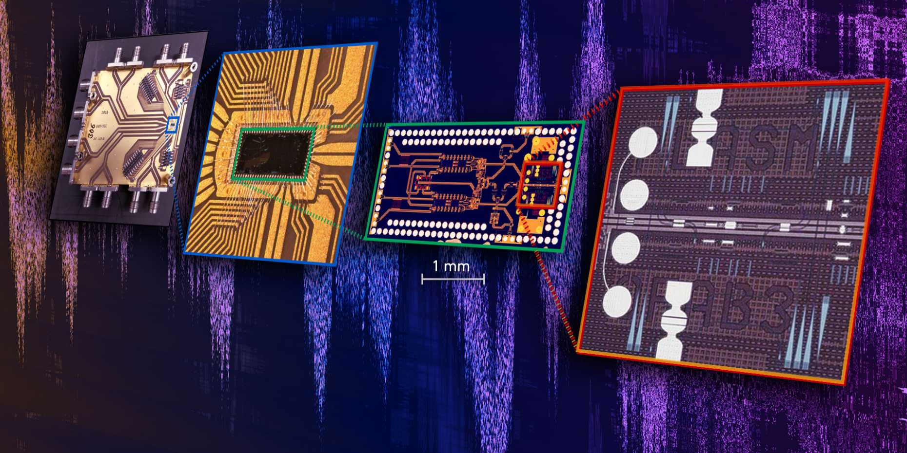 The new, highly compact chip brings together the fastest electronic and light-based elements in a single component for the first time. (Image: ETH Zurich/Nature Electronics)
Researchers from ETH Zurich have achieved what scientists have been attempting to do for some 20 years: in their laboratory work as part of European Horizon 2020 research projects, they have manufactured a chip on which fast electronic signals can be converted directly into ultrafast light signals – with practically no loss of signal quality. This represents a significant breakthrough in terms of the efficiency of optical communication infrastructures that use light to transmit data, such as fibre optic networks.
In cities like Zurich, these fibre optic networks are already being used to deliver high-speed internet, digital telephony, TV, and network-based video or audio services (“streaming”). However, by the end of this decade, even these optical communication networks may reach their limits when it comes to rapid data transmission.
This is due to the growing demand for online services for streaming, storage and computation, as well as the advent of artificial intelligence and 5G networks. Today’s optical networks achieve data transmission rates in the region of gigabits (109 bits) per second. The limit is around 100 gigabits per lane und wavelength. In the future, however, transmission rates will need to reach the terabit region (1012 bits per second).
New: electronics and light on the same chip
“The rising demand will call for new solutions,” says Juerg Leuthold, ETH Professor of Photonics and Communications. “The key to this paradigm shift lies in combining electronic and photonic elements on a single chip.” The field of photonics (the science of light particles) studies optical technologies for the transmission, storage and processing of information.
The ETH researchers have now achieved precisely this combination: in an experiment performed in collaboration with partners in Germany, the US, Israel and Greece, they were able to bring together electronic and light-based elements on one and the same chip for the first time. This is a huge step from a technical perspective, because these elements currently have to be manufactured on separate chips and then connected up with wires.
There are consequences to this approach: on the one hand, manufacturing the electronic and photonic chips separately is expensive. On the other hand, it hampers performance during the conversion of electronic signals into light signals and thereby limits the transmission speed in fibre optic communication networks, explains Ueli Koch, a postdoc in Leuthold’s group and lead author of the study, which was published in the journal Nature Electronics.
Compact size for maximum speed
“If you convert the electronic signals into light signals using separate chips, you lose a significant amount of signal quality. This also limits the speed of data transmission using light,” says Koch. His approach therefore begins with the modulator, a component on the chip that generates light of a given intensity by converting the electrical signals into light waves. The size of the modulator must be as small as possible in order to avoid a loss of quality and intensity in the conversion process, and in order to transmit the light – or rather the data – faster than is possible today (see ETH News, 01.02.2016).

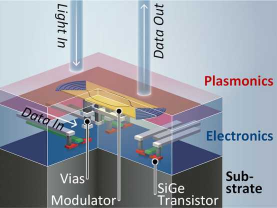
Thanks to the combination of electronics and plasmonics on a single chip, light signals can be amplified and data can be transmitted faster. (Graphic: IEF/Springer Nature Ltd.)
This compactness is achieved by placing the electronic and photonic components tightly on top of one another, like two layers, and connecting them directly to the chip by means of “on-chip vias”. This layering of the electronics and photonics shortens transmission paths and reduces losses in terms of signal quality. As the electronics and photonics are implemented on one single substrate, the researchers describe this approach as “monolithic co-integration”.
For the past 20 years, the monolithic approach has failed because photonic chips are much bigger than electronic ones. This prevented them from being combined on a single chip, says Juerg Leuthold. The size of the photonic elements makes it impossible to combine them with the metal oxide semiconductor (CMOS) technology that is prevalent in electronics today.
Plasmonics: magic potion for semiconductor chips
“We’ve now overcome the size difference between photonics and electronics by replacing the photonics with plasmonics,” says Leuthold. For ten years, scientists have been predicting that plasmonics, which is a branch of photonics, could provide the foundation for ultrafast chips. Plasmonics can be used to squeeze light waves into structures that are much smaller than the wavelength of the light (see ETH News, 18.11.2019).
As the plasmonic chips are smaller than electronic ones, it is now actually possible to manufacture much more compact, monolithic chips that incorporate both a photonic and an electronic layer. In order to then convert the electrical signals into even faster optical ones, the photonic layer (seen in red in the graphic) contains a plasmonic intensity modulator. This is based on metal structures that channel the light in order to reach higher speeds.
Combined for record speed
This is in addition to a speed increase in the electronic layer (seen in blue in the graphic). In a process known as “4:1 multiplexing”, four lower-speed input signals are bundled and amplified so that, together, they form a high-speed electrical signal. “This is then converted into a high-speed optical signal,” says Koch. “In this way, we were able to transmit data on a monolithic chip at a speed of over 100 gigabits per second for the first time.”
In order to reach this record-breaking speed, the researchers combined plasmonics not only with classical CMOS electronics but also with the even faster BiCMOS technology. They also made use of a new temperature-stable, electro-optical material from the University of Washington as well as insights from the Horizon 2020 projects PLASMOfab and plaCMOS. According to Leuthold, their experiment showed that these technologies can be combined to create one of the fastest compact chips: “We’re convinced that this solution can also pave the way for faster data transmission in optical communication networks of the future.”
Reference
Koch, U., Uhl, C., Hettrich, H. et al. A monolithic bipolar CMOS electronic–plasmonic high-speed transmitter. Nature Electronics 3, 338–345 (2020). DOI: 10.1038/s41928-020-0417-9
Koch, U. A monolithic bipolar CMOS electronic plasmonic high-speed transmitter. Nature Research Device & Materials Engineering, Behind the Paper. devicematerialscommunity.nature.com/users/407225-ueli-koch/posts/a-monolithic-bipolar-cmos-electronic-plasmonic-high-speed-transmitter
Moazeni, S. CMOS and plasmonics get close. Nature Electronics 3, 302–303 (2020). DOI: 10.1038/s41928-020-0426-8


