2025-12-04 東京科学大学

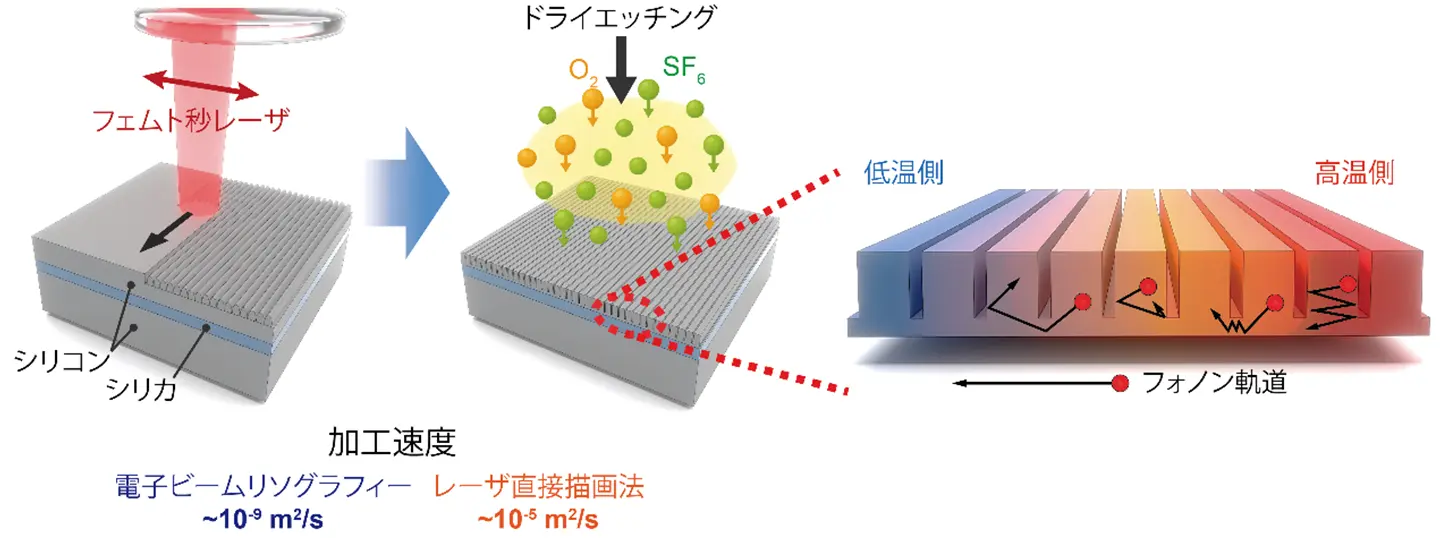
図1. レーザ直接描画法とドライエッチングによるナノ周期構造の形成とフォノンの振る舞い
<関連情報>
- https://www.isct.ac.jp/ja/news/le6e1jgyrrfk
- https://advanced.onlinelibrary.wiley.com/doi/10.1002/adfm.202525269
フェムト秒レーザー直接描画フォノニックナノ構造によるスケーラブルな熱工学 Scalable Thermal Engineering via Femtosecond Laser-Direct-Written Phononic Nanostructures
Hiroki Hamma, Roman Anufriev, Kazuyoshi Fushinobu, Masahiro Nomura, Byunggi Kim
Advanced Functional Materials Published: 03 December 2025
DOI:https://doi.org/10.1002/adfm.202525269
Abstract
Modern electronics demands innovative thermal management strategy beyond conventional approaches. Here, A transformative platform bridging laboratory-scale phononic nanostructures and industrial-scale thermal engineering is demonstrated via femtosecond laser-induced periodic surface structures (fs-LIPSS). Laser-direct-written phononic metamaterials is achieved with throughputs exceeding 10−⁵ m2 s−1—three orders of magnitude faster than electron beam lithography—while maintaining nanoscale resolution. Applied to silicon membranes, the fs-LIPSS reduce thermal conductivity from 101 to 76 W m−1 K−1, surpassing thin-film limit predicted by Fuchs–Sondheimer model. Monte Carlo simulations corroborate these findings, showing that long mean free paths are limited by the fs-LIPSS, while ablation-induced roughness mediates isotropic modulation of thermal conductivity via enhanced diffuse scattering. Thus, this maskless and resist-free process enables the fabrication of phononic nanostructures that are CMOS-compatible and scalable to wafer-level dimensions. This work establishes the fs-LIPSS as a versatile approach that makes phonon engineering practical for real-world devices, unlocking applications in quantum technologies, on-chip energy conversion, and high-performance computing.


