2025-10-17 デューク大学
Web要約 の発言:
<関連情報>
- https://pratt.duke.edu/news/submicrometer-transistor-printing/
- https://www.nature.com/articles/s41928-025-01470-7
- https://ieeexplore.ieee.org/document/10713360
- https://www.nature.com/articles/s41928-021-00574-0
サブミクロンカーボンナノチューブトランジスタの毛細管フロー印刷 Capillary flow printing of submicrometre carbon nanotube transistors
Brittany N. Smith,Faris M. Albarghouthi,James L. Doherty,Xuancheng Pei,Quentin Macfarlane,Matthew Salfity,Daniel Badia,Marc Pascual,Pascal Boncenne,Nathan Bigan,Amin M’Barki & Aaron D. Franklin
Nature Electronics Published:17 October 2025
DOI:https://doi.org/10.1038/s41928-025-01470-7

Abstract
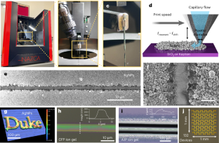
Printed transistors have a wide range of applications, but the limited resolution of printing techniques (10–30 µm) has been a barrier to utility and scalability. Printed submicrometre channel lengths have previously been achieved. However, this has required chemical processes or tedious post-processing, which limits applicability. Here we show that capillary flow printing can create submicrometre carbon nanotube thin-film transistors without chemical modification or physical manipulation after printing. We show that the approach can be used to print conducting, semiconducting and insulating inks on different types of substrate (silicon, Kapton and paper), and can be used to fabricate various thin-film transistor device architectures. The printed carbon nanotube thin-film transistors exhibit on-currents of 1.12 mA mm−1 when back gated on Si/SiO2 and 490 µA mm−1 when side gated through ion gel on Kapton. We also show that devices printed on Kapton offer mechanical bending and sweep rate resilience, illustrating the potential of these printed devices for flexible applications.
プリントカーボンベースのリサイクル可能なトランジスタバックプレーンを備えた液晶ディスプレイ Liquid Crystal Displays With Printed Carbon-Based Recyclable Transistor Backplanes
James L. Doherty; Ye Zhang; Brittany N. Smith; Hansel Alex Hobbie; Ioannis Kymissis; Aaron D. Franklin
IEEE Electron Device Letters Published:10 October 2024
DOI:https://doi.org/10.1109/LED.2024.3477434
Abstract
We report the first demonstration of displays driven by embedded transistors that were additively manufactured entirely by aerosol jet printing. The backplanes of the liquid crystal displays (LCDs) consist of transistors printed from graphene, carbon nanotubes, and crystalline nanocellulose onto a glass substrate with prepatterned indium tin oxide electrodes. We addressed challenges of integrating fully printed devices into both the crossbar array structure and layered vertical structure required for an LCD, showing successful pixel switching at up to 60 Hz. As these thin-film transistors are printed exclusively from carbon-based recyclable materials, without high temperatures or vacuum processing, they offer a promising means for reducing waste in future display technologies.
結晶ナノセルロース誘電体を用いた印刷可能かつリサイクル可能なカーボンエレクトロニクス Printable and recyclable carbon electronics using crystalline nanocellulose dielectrics
Nicholas X. Williams,George Bullard,Nathaniel Brooke,Michael J. Therien & Aaron D. Franklin
Nature Electronics Published:26 April 2021
DOI:https://doi.org/10.1038/s41928-021-00574-0
Abstract
Electronic waste can lead to the accumulation of environmentally and biologically toxic materials and is a growing global concern. Developments in transient electronics—in which devices are designed to disintegrate after use—have focused on increasing the biocompatibility, whereas efforts to develop methods to recapture and reuse materials have focused on conducting materials, while neglecting other electronic materials. Here, we report all-carbon thin-film transistors made using crystalline nanocellulose as a dielectric, carbon nanotubes as a semiconductor, graphene as a conductor and paper as a substrate. A crystalline nanocellulose ink is developed that is compatible with nanotube and graphene inks and can be written onto a paper substrate using room-temperature aerosol jet printing. The addition of mobile sodium ions to the dielectric improves the thin-film transistor on-current (87 μA mm−1) and subthreshold swing (132 mV dec−1), and leads to a faster voltage sweep rate (by around 20 times) than without ions. The devices also exhibit stable performance over six months in ambient conditions and can be controllably decomposed, with the graphene and carbon nanotube inks recaptured for recycling (>95% recapture efficiency) and reprinting of new transistors. We demonstrate the utility of the thin-film transistors by creating a fully printed, paper-based biosensor for lactate sensing.


