2023-07-16 カリフォルニア工科大学(Caltech)
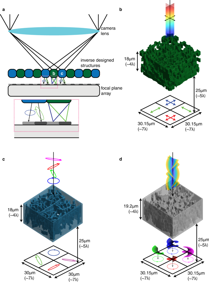
◆研究では可視光でも使用可能な小型デバイスが開発され、カメラのセンサの直上に配置し、赤、緑、青の光を別々のピクセルに誘導できます。この技術は実証段階ですが、さらなる研究により実用的な製造技術に進展する可能性があります。
<関連情報>
- https://www.caltech.edu/about/news/evolving-and-3d-printing-new-nanoscale-optical-devices
- https://www.nature.com/articles/s41467-023-38258-2
3Dパターン逆デザイン中赤外メタオプティクス 3D-patterned inverse-designed mid-infrared metaoptics
Gregory Roberts,Conner Ballew,Tianzhe Zheng,Juan C. Garcia,Sarah Camayd-Muñoz,Philip W. C. Hon & Andrei Faraon
Nature Communications Published:13 May 2023
DOI:https://doi.org/10.1038/s41467-023-38258-2

Abstract
Modern imaging systems can be enhanced in efficiency, compactness, and application through the introduction of multilayer nanopatterned structures for manipulation of light based on its fundamental properties. High transmission multispectral imaging is elusive due to the commonplace use of filter arrays which discard most of the incident light. Further, given the challenges of miniaturizing optical systems, most cameras do not leverage the wealth of information in polarization and spatial degrees of freedom. Optical metamaterials can respond to these electromagnetic properties but have been explored primarily in single-layer geometries, limiting their performance and multifunctional capacity. Here we use advanced two-photon lithography to realize multilayer scattering structures that achieve highly nontrivial optical transformations intended to process light just before it reaches a focal plane array. Computationally optimized multispectral and polarimetric sorting devices are fabricated with submicron feature sizes and experimentally validated in the mid-infrared. A final structure shown in simulation redirects light based on its angular momentum. These devices demonstrate that with precise 3-dimensional nanopatterning, one can directly modify the scattering properties of a sensor array to create advanced imaging systems.


