2025-12-03 サンディア国立研究所(SNL)

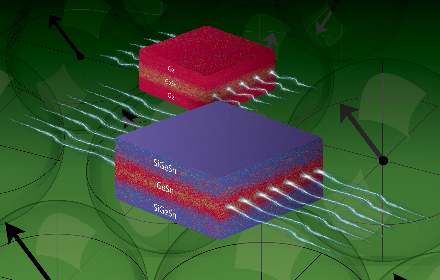
An illustration of two quantum wells. Researchers found that by adding small amounts of silicon and tin to the outer barriers, they increased the mobility of charge carriers passing through the middle. (Image courtesy of the University of Arkansas) Click on the thumbnail for a high-resolution image.
<関連情報>
- https://newsreleases.sandia.gov/quantum-computers-get-a-boost-from-a-tiny-material-tweak/
- https://advanced.onlinelibrary.wiley.com/doi/full/10.1002/aelm.202500460
SiGeSn障壁を有するGeSn量子井戸における高移動度と静電気 High Mobility and Electrostatics in GeSn Quantum Wells With SiGeSn Barriers
Christopher R. Allemang, David Lidsky, Peter Sharma, Shang Liu, Jifeng Liu, Yunsheng Qiu, Shuiqing Yu, Tzu-Ming Lu
Advanced Electronic Materials Published: 09 October 2025
DOI:https://doi.org/10.1002/aelm.202500460
Abstract
GeSn is an emerging material with potential applications in next-generation integrated optoelectronics and quantum information processing. While GeSn/SiGeSn quantum wells exhibit promising optical properties, their electrical transport characteristics and governing electrostatics in gated structures remain unexplored. Heterostructure field-effect transistors are fabricated using GeSn/SiGeSn quantum wells and electronic transport properties of 2D holes are characterized. At 2 K, heterostructure field-effect transistors with well/barrier compositions of Ge0.945Sn0.055/Si0.03Ge0.93Sn0.04 and Ge0.9Sn0.1/Si0.017Ge0.927Sn0.056, show peak mobilities of 9000 and 19 000 cm2/Vs, respectively, the latter setting a record for the highest mobility reported for GeSn quantum wells with a Sn concentration around 6 % or greater. Remarkably, at low carrier densities, devices with a SiGeSn barrier exhibit mobilities several times higher than previously reported for GeSn quantum wells with a Ge barrier. This higher mobility contrasts with the expectation that alloy scattering from the barrier would reduce carrier mobility. Two mechanisms based on atom probe tomography data analyses are proposed: i) unintentionally improved SiGeSn/GeSn interface and/or ii) reduced alloy scattering from short-range order. Significant current–voltage hysteresis is observed, with the effective threshold gate voltage shifting by more than 5 V, attributed to non-equilibrium trapped charge at various interfaces within the SiGeSn heterostructure.


