2025-07-24 ファインセラミックスセンター,科学技術振興機構

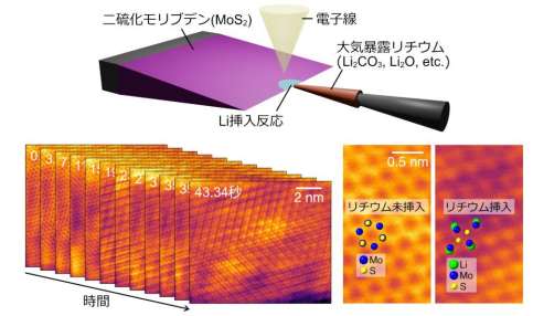
図1 本研究の概要
<関連情報>
- https://www.jst.go.jp/pr/announce/20250724-2/index.html
- https://www.jst.go.jp/pr/announce/20250724-2/pdf/20250724-2.pdf
- https://pubs.acs.org/doi/10.1021/acsnano.5c05218
リチウム化中のMoS2における原子スケールでのイン・シチュ走査透過電子顕微鏡観察 Atomic-Scale In Situ Scanning Transmission Electron Microscopy of MoS2 during Lithiation
Kei Nakayama,and Shunsuke Kobayashi
ACS Nano Published: July 21, 2025
DOI:https://doi.org/10.1021/acsnano.5c05218
Abstract
Atomic-scale in situ characterization techniques are necessary to clarify the dynamic local structural changes during intercalation reactions. High-resolution transmission electron microscopy (HRTEM) is at the forefront of this field. However, the image contrast in HRTEM is not always straightforward, necessitating the exploration of alternative imaging techniques. Here, using annular dark-field (ADF) scanning transmission electron microscopy (STEM), which is expected to provide a more directly interpretable image contrast, we report atomic-scale in situ observation of the MoS2 lithiation process induced by electron irradiation. Using a single-crystalline specimen, dedicated specimen holder, and alternate low- and high-magnification image acquisition technique, a time series of ADF-STEM images was recorded at a frame rate of 1 fps, followed by image filtering. Consequently, successive changes in the domain structure were clarified, starting with an anisotropically expanding structural phase transition, followed by the disappearance and formation of domains with different crystal orientations, which were attributed to changes in the internal stress and interfacial energy.


