2025-07-14 ノースウェスタン大学

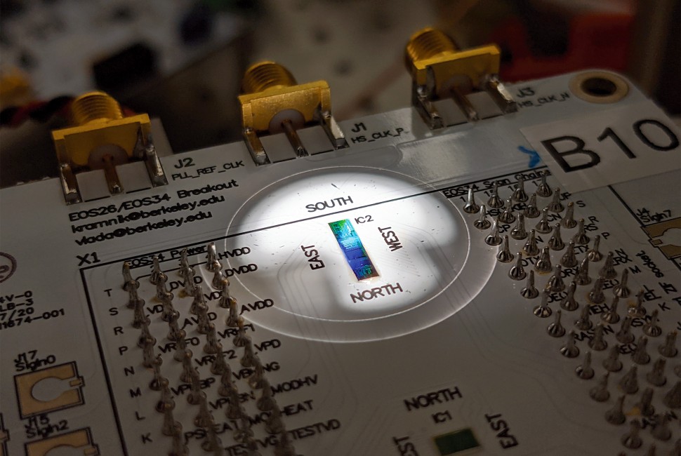
A packaged circuit board containing the chip placed under microscope in probe station during an experiment. The first-of-its-kind silicon chip combines both the quantum light-generating components (photonics) with classical electronic control circuits — all packed into an area measuring just one millimeter by one millimeter.
<関連情報>
- https://news.northwestern.edu/stories/2025/07/first-electronic-photonic-quantum-chip-manufactured-in-commercial-foundry/
- https://www.nature.com/articles/s41928-025-01410-5
- https://opg.optica.org/oe/fulltext.cfm?uri=oe-14-25-12388&id=119785
CMOSチップ上での量子光源のスケーラブルなフィードバック安定化 Scalable feedback stabilization of quantum light sources on a CMOS chip
Danielius Kramnik,Imbert Wang,Anirudh Ramesh,Josep M. Fargas Cabanillas,Ðorđe Gluhović,Sidney Buchbinder,Panagiotis Zarkos,Christos Adamopoulos,Prem Kumar,Vladimir M. Stojanović & Miloš A. Popović
Nature Electronics Published:14 July 2025
DOI:https://doi.org/10.1038/s41928-025-01410-5
Abstract
Silicon photonics could soon be used to create the vast numbers of physical qubits needed to achieve useful quantum information processing by leveraging mature complementary metal–oxide–semiconductor (CMOS) manufacturing to miniaturize optical devices for generating and manipulating quantum states of light. However, the development of practical silicon quantum-photonic integrated circuits faces challenges related to high sensitivity to process and temperature variations, free-carrier and self-heating nonlinearities, and thermal crosstalk. These issues have been partially addressed with bulky off-chip electronics, but this sacrifices many benefits of a chip-scale platform. Here we report an electronic–photonic quantum system-on-chip that consists of quantum-correlated photon-pair sources stabilized via on-chip feedback control circuits and is fabricated in a commercial 45-nm CMOS microelectronics foundry. We use non-invasive photocurrent sensing in a tunable microring cavity photon-pair source to actively lock it to a fixed-wavelength pump laser while operating in the quantum regime, enabling large-scale microring-based quantum systems. We also show that these sources maintain stable quantum properties and operate reliably in a practical setting with many adjacent photon-pair sources creating thermal disturbances on the same chip. Such dense integration of electronics and photonics enables implementation and control of quantum-photonic systems at the scale needed to achieve useful quantum information processing with CMOS-fabricated chips.
ナノスケールのシリコン導波路における相関光子の生成 Generation of correlated photons in nanoscale silicon waveguides
Jay E. Sharping, Kim Fook Lee, Mark A. Foster, Amy C. Turner, Bradley S. Schmidt, Michal Lipson, Alexander L. Gaeta, and Prem Kumar
Optics Express Published: December 11, 2006
DOI:https://doi.org/10.1364/OE.14.012388
Abstract
We experimentally study the generation of correlated pairs of photons through four-wave mixing (FWM) in embedded silicon waveguides. The waveguides, which are designed to exhibit anomalous group-velocity dispersion at wavelengths near 1555 nm, allow phase matched FWM and thus efficient pair-wise generation of non-degenerate signal and idler photons. Photon counting measurements yield a coincidence-to-accidental ratio (CAR) of around 25 for a signal (idler) photon production rate of about 0.05 per pulse. We characterize the variation in CAR as a function of pump power and pump-to-sideband wavelength detuning. These measurements represent a first step towards the development of tools for quantum information processing which are based on CMOS-compatible, silicon-on-insulator technology.


