2024-12-18 マサチューセッツ工科大学
<関連情報>
- https://news.mit.edu/2024/mit-engineers-grow-high-rise-3d-chips-1218
- https://www.nature.com/articles/s41586-024-08236-9
- https://tiisys.com/blog/2023/01/20/post-115664/
単結晶2次元半導体の成長に基づくモノリシック3次元集積化 Growth-based monolithic 3D integration of single-crystal 2D semiconductors
Ki Seok Kim,Seunghwan Seo,Junyoung Kwon,Doyoon Lee,Changhyun Kim,Jung-El Ryu,Jekyung Kim,Jun Min Suh,Hang-Gyo Jung,Youhwan Jo,June-Chul Shin,Min-Kyu Song,Jin Feng,Hogeun Ahn,Sangho Lee,Kyeongjae Cho,Jongwook Jeon,Minsu Seol,Jin-Hong Park,Sang Won Kim & Jeehwan Kim
Nature Published:18 December 2024
DOI:https://doi.org/10.1038/s41586-024-08236-9

Abstract
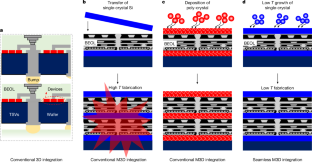
The demand for the three-dimensional (3D) integration of electronic components is steadily increasing. Despite substantial processing challenges, the through-silicon-via (TSV) technique emerges as the only viable method for integrating single-crystalline device components in a 3D format1,2. Although monolithic 3D (M3D) integration schemes show promise3, the seamless connection of single-crystalline semiconductors without intervening wafers has yet to be demonstrated. This challenge arises from the inherent difficulty of growing single crystals on amorphous or polycrystalline surfaces after the back-end-of-the-line process at low temperatures to preserve the underlying circuitry. Consequently, a practical growth-based solution for M3D of single crystals remains unknown. Here we present a method for growing single-crystalline channel materials, specifically composed of transition metal dichalcogenides, on amorphous and polycrystalline surfaces at temperatures low enough to preserve the underlying electronic components. Building on this developed technique, we demonstrate the seamless monolithic integration of vertical single-crystalline logic transistor arrays. This accomplishment leads to the development of unprecedented vertical complementary metal oxide semiconductor (CMOS) arrays composed of grown single-crystalline channels. Ultimately, this achievement provides opportunities for M3D integration of various electronic hardware in the form of single crystals.


