2024-07-03 韓国基礎科学研究院(IBS)
<関連情報>
- https://www.ibs.re.kr/cop/bbs/BBSMSTR_000000000738/selectBoardArticle.do
- https://www.nature.com/articles/s41565-024-01706-1
超スケール2次元MoS2電界効果トランジスタのための集積化1次元エピタキシャルミラー双晶境界 Integrated 1D epitaxial mirror twin boundaries for ultrascaled 2D MoS2 field-effect transistors
Heonsu Ahn,Gunho Moon,Hang-gyo Jung,Bingchen Deng,Dong-Hwan Yang,Sera Yang,Cheolhee Han,Hyunje Cho,Youngki Yeo,Cheol-Joo Kim,Chan-Ho Yang,Jonghwan Kim,Si-Young Choi,Hongkun Park,Jongwook Jeon,Jin-Hong Park & Moon-Ho Jo
Nature Nanotechnology Published:03 July 2024
DOI:https://doi.org/10.1038/s41565-024-01706-1

Abstract
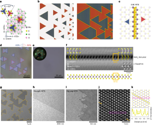
In atomically thin van der Waals materials, grain boundaries—the line defects between adjacent crystal grains with tilted in-plane rotations—are omnipresent. When the tilting angles are arbitrary, the grain boundaries form inhomogeneous sublattices, giving rise to local electronic states that are not controlled. Here we report on epitaxial realizations of deterministic MoS2 mirror twin boundaries (MTBs) at which two adjoining crystals are reflection mirroring by an exactly 60° rotation by position-controlled epitaxy. We showed that these epitaxial MTBs are one-dimensionally metallic to a circuit length scale. By utilizing the ultimate one-dimensional (1D) feature (width ~0.4 nm and length up to a few tens of micrometres), we incorporated the epitaxial MTBs as a 1D gate to build integrated two-dimensional field-effect transistors (FETs). The critical role of the 1D MTB gate was verified to scale the depletion channel length down to 3.9 nm, resulting in a substantially lowered channel off-current at lower gate voltages. With that, in both individual and array FETs, we demonstrated state-of-the-art performances for low-power logics. The 1D epitaxial MTB gates in this work suggest a novel synthetic pathway for the integration of two-dimensional FETs—that are immune to high gate capacitance—towards ultimate scaling.


