2024-07-01 米国国立再生可能エネルギー研究所(NREL)
<関連情報>
- https://www.nrel.gov/news/press/2024/optoelectronics-gain-spin-control-from-chiral-perovskites-and-iii-v-semiconductors.html
- https://www.nature.com/articles/s41586-024-07560-4
キラルペロブスカイト/III-V界面を介した室温スピン注入 Room-temperature spin injection across a chiral perovskite/III–V interface
Matthew P. Hautzinger,Xin Pan,Steven C. Hayden,Jiselle Y. Ye,Qi Jiang,Mickey J. Wilson,Alan J. Phillips,Yifan Dong,Emily K. Raulerson,Ian A. Leahy,Chun-Sheng Jiang,Jeffrey L. Blackburn,Joseph M. Luther,Yuan Lu,Katherine Jungjohann,Z. Valy Vardeny,Joseph J. Berry,Kirstin Alberi & Matthew C. Beard
Nature Published:19 June 2024
DOI:https://doi.org/10.1038/s41586-024-07560-4

Abstract
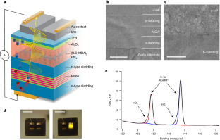
Spin accumulation in semiconductor structures at room temperature and without magnetic fields is key to enable a broader range of optoelectronic functionality1. Current efforts are limited owing to inherent inefficiencies associated with spin injection across semiconductor interfaces2. Here we demonstrate spin injection across chiral halide perovskite/III–V interfaces achieving spin accumulation in a standard semiconductor III–V (AlxGa1−x)0.5In0.5P multiple quantum well light-emitting diode. The spin accumulation in the multiple quantum well is detected through emission of circularly polarized light with a degree of polarization of up to 15 ± 4%. The chiral perovskite/III–V interface was characterized with X-ray photoelectron spectroscopy, cross-sectional scanning Kelvin probe force microscopy and cross-sectional transmission electron microscopy imaging, showing a clean semiconductor/semiconductor interface at which the Fermi level can equilibrate. These findings demonstrate that chiral perovskite semiconductors can transform well-developed semiconductor platforms into ones that can also control spin.


